From Schematic to PCB
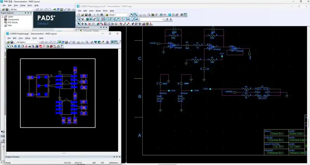
I first traced how Logic nets reach footprints in Layout, then reread the screen as schematic, package mapping, net transfer, placement, routing, and checks.
Engineering Study Track
I use my saved Decal Wizard and PPG design screens to rebuild the part, schematic, placement, and checking workflow.
The PADS captures are my saved work screens. KiCad and Siemens documents are linked only when comparing equivalent concepts.
8 Topics
I first traced how Logic nets reach footprints in Layout, then reread the screen as schematic, package mapping, net transfer, placement, routing, and checks.
Treating schematic symbols, pin names, electrical roles, and PCB geometry as one object makes revisions brittle. I separated the logical part from its physical decal.
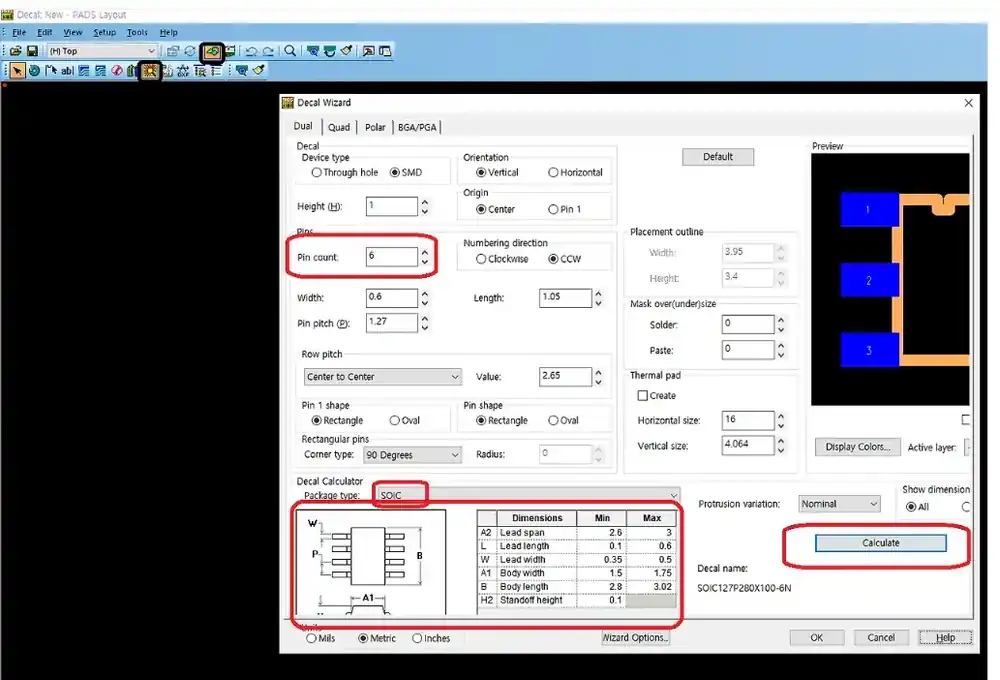
I checked pin count, pitch, pad width and length, and row spacing one by one, then wrote down a datasheet-first comparison instead of trusting the package name.
I followed the feedback resistors and capacitors around the OPA2333 stages and marked each input and output. I treat the Layout capture as a saved placement view, not proof of completed routing.
I reframed placement as shortening current loops and sensitive analog paths rather than filling space, checking connectors, amplifier stages, and bypass capacitors in that order.
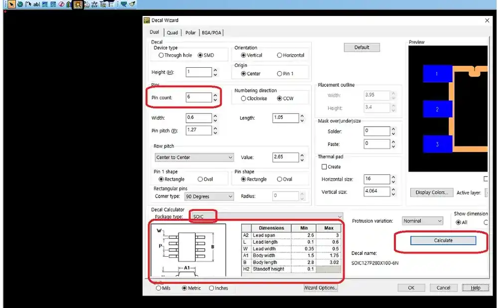
I started with pad, mask, clearance, drill, and outline rules. Gerber and drill outputs belong after DRC, so a setup screen alone is not presented as fabrication-ready work.
PADS decals and KiCad footprints play similar roles but use different file and library structures. I compare pads, pins, courtyards, and 3D models without implying file compatibility.
I finish by comparing schematic and placement for pin mapping, power, feedback loops, and orientation, stopping at what the saved screen actually shows.