PADS · PCB Design · 05
Placement and Signal Paths
I reframed placement as shortening current loops and sensitive analog paths rather than filling space, checking connectors, amplifier stages, and bypass capacitors in that order.
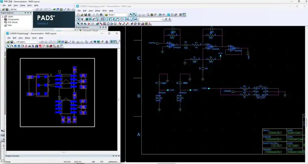
What I checked first
I reframed placement as shortening current loops and sensitive analog paths rather than filling space, checking connectors, amplifier stages, and bypass capacitors in that order.
Source view
Verified image and track references are used here.
Implementation path
Only the saved configuration and processing sequence are shown.
Key terms
- return path
- analog routing
- decoupling
- connectors
Review sequence
- return path
- analog routing → decoupling
- connectors
Official references
The PADS captures are my saved work screens. KiCad and Siemens documents are linked only when comparing equivalent concepts.