PADS · PCB Design · 04
Reading the PPG Analog Front End
I followed the feedback resistors and capacitors around the OPA2333 stages and marked each input and output. I treat the Layout capture as a saved placement view, not proof of completed routing.
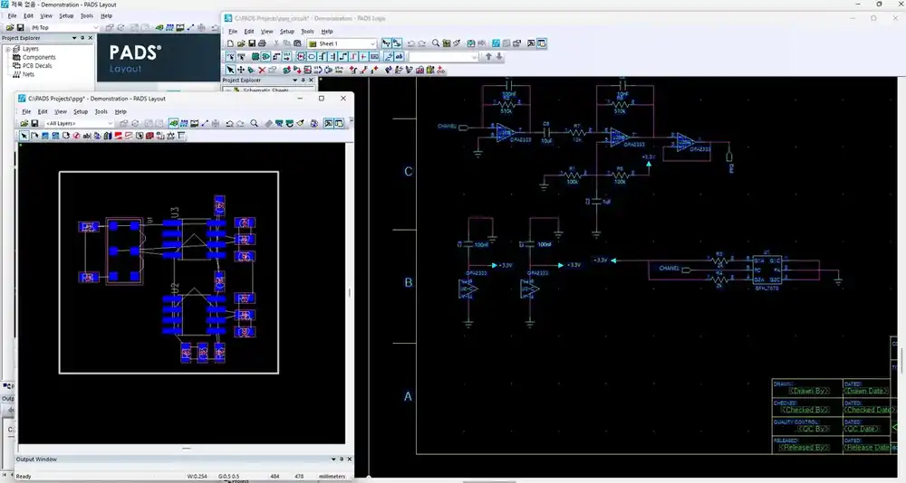
What I checked first
I followed the feedback resistors and capacitors around the OPA2333 stages and marked each input and output. I treat the Layout capture as a saved placement view, not proof of completed routing.
Source view
Verified image and track references are used here.
Implementation path
Only the saved configuration and processing sequence are shown.
Key terms
- op-amp stage
- feedback
- decoupling
- signal path
Review sequence
- op-amp stage
- feedback → decoupling
- signal path
Official references
The PADS captures are my saved work screens. KiCad and Siemens documents are linked only when comparing equivalent concepts.