PADS · PCB Design · 01
From Schematic to PCB
I first traced how Logic nets reach footprints in Layout, then reread the screen as schematic, package mapping, net transfer, placement, routing, and checks.
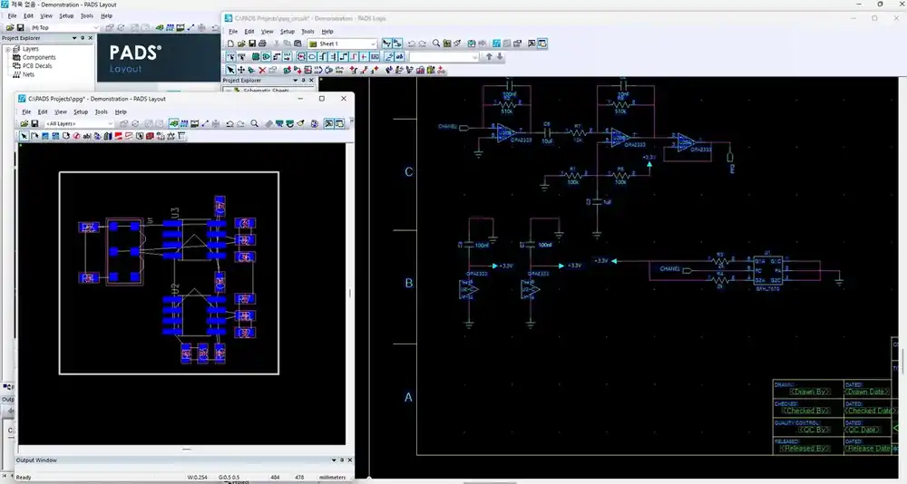
What I checked first
I first traced how Logic nets reach footprints in Layout, then reread the screen as schematic, package mapping, net transfer, placement, routing, and checks.
Source view
Verified image and track references are used here.
Implementation path
Only the saved configuration and processing sequence are shown.
Key terms
- schematic
- package mapping
- netlist
- placement
Review sequence
- schematic
- package mapping → netlist
- placement
Official references
The PADS captures are my saved work screens. KiCad and Siemens documents are linked only when comparing equivalent concepts.