PADS · PCB Design · 08
Reviewing the PPG Board Screen
I finish by comparing schematic and placement for pin mapping, power, feedback loops, and orientation, stopping at what the saved screen actually shows.
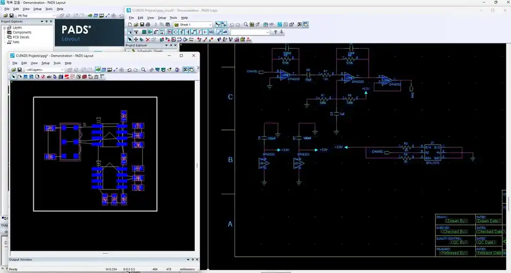
What I checked first
I finish by comparing schematic and placement for pin mapping, power, feedback loops, and orientation, stopping at what the saved screen actually shows.
Source view
Verified image and track references are used here.
Implementation path
Only the saved configuration and processing sequence are shown.
Key terms
- cross-probing
- orientation
- power integrity
- review checklist
Review sequence
- cross-probing
- orientation → power integrity
- review checklist
Official references
The PADS captures are my saved work screens. KiCad and Siemens documents are linked only when comparing equivalent concepts.