Completed a fabrication handoff from KiCad source through Gerber and drill files
Architecture and result views
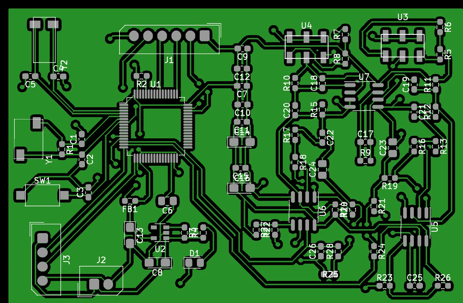
Power, clock, debug, and communication control logic extracted from STM.schSensor-to-ADC signal chain for both PPG channels identified in Analog.schKiCad footprint and decal set for the MCU, sensors, op amps, and LDOEnlarged MCU, clock, power, debug-interface placement, and fan-out routingEnlarged analog-front-end placement grouping the sensors, input networks, and active-filter stagesFront copper, mask, and silkscreen layers rendered directly from the fabrication GerbersBottom-side ground copper used for signal return paths
What I worked on
Built STM32F411RETx power, clock, SWD, and UART circuitry
Laid out two SFH7070 inputs and OPA2333-based low-noise analog paths
Added a bottom ground plane, routed two layers, and generated fabrication files
Code and results
KiCad hierarchical schematic and PCB source
Front/back copper, mask, paste, and silkscreen Gerbers
PTH/NPTH drill and Gerber job files
Design scope and next steps
Available artifacts: schematics, routing, and fabrication outputs. Follow-up measurements: PPG waveforms, SNR, filter cutoff, and biosignal accuracy.
Two SFH7070 sensor signals pass through OPA2333 amplification/filter stages into STM32F411 ADC A0/A1. The two-layer board includes a 5-V input, 3.3-V LDO, 8-MHz/32.768-kHz clocks, SWD, UART, and bottom-side ground copper.