STM32 · Sensor Acquisition
From Analog Front End to Fabrication Files on an STM32F411 PPG PCB
2026-09-04 · updated 2026-09-04 · Hyeongrok Ryu
A two-layer KiCad design connecting SFH7070 sensors, OPA2333 front ends, STM32F411, and a complete Gerber package.
- Type / level
- project-log · advanced
- Tools
- KiCad, STM32F411RETx, SFH7070, OPA2333, SPX3819, Gerber
Architecture
The board places two SFH7070 optical sensors, three dual OPA2333 amplifiers, an STM32F411RETx, and power, clock, debug, and UART circuitry on one PCB. Hierarchical STM and Analog sheets make it possible to follow the MCU support circuits and small-signal analog paths separately.
SFH7070 x2 -> OPA2333 amplification/filter -> STM32F411 ADC A0/A1 -> UART
5 V input  -> SPX3819 3.3 V rail            -> analog and digital circuits
PPG analog front end
Each sensor output passes through an OPA2333-based amplification/filter stage and reaches MCU ADC input A0 or A1. A zero-drift amplifier is a useful choice for reducing offset in small DC and low-frequency signals, but the part name alone does not establish noise or bandwidth. Gain and RC networks still need to be traced channel by channel in the schematic.
MCU and interfaces
The STM32F411RETx is supported by an SPX3819 regulator from 5 V to 3.3 V, an 8-MHz main clock, and a 32.768-kHz clock. SWD provides programming/debug access, while UART supports data inspection. Because analog inputs, clocks, and serial signals meet at one MCU, I compared pin mapping and decoupling in both the schematic and PCB.
Two-layer layout
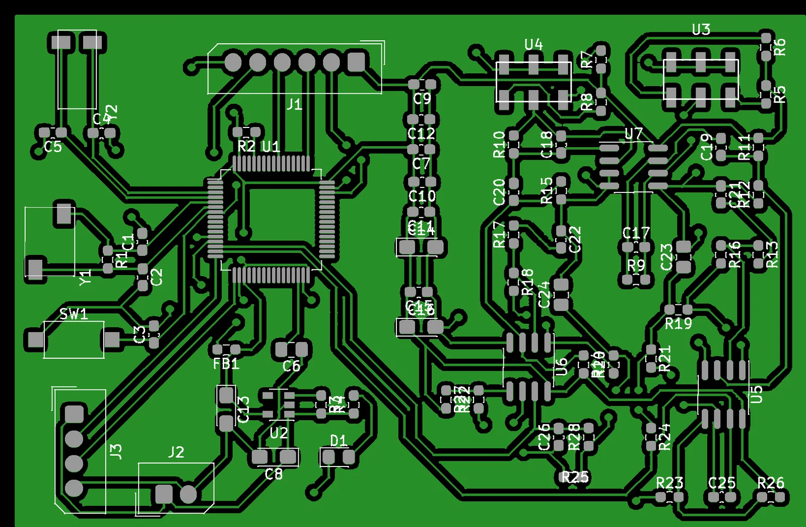
The board is approximately 80.6 × 52.2 mm and contains 69 modules, 83 nets, 602 tracks, and 56 plated holes. The front side carries the MCU, sensor interfaces, amplifiers, and connectors; the bottom uses broad ground copper. Short analog input routes, return paths, and separation from clocks and digital edges were the main review points.
Fabrication outputs
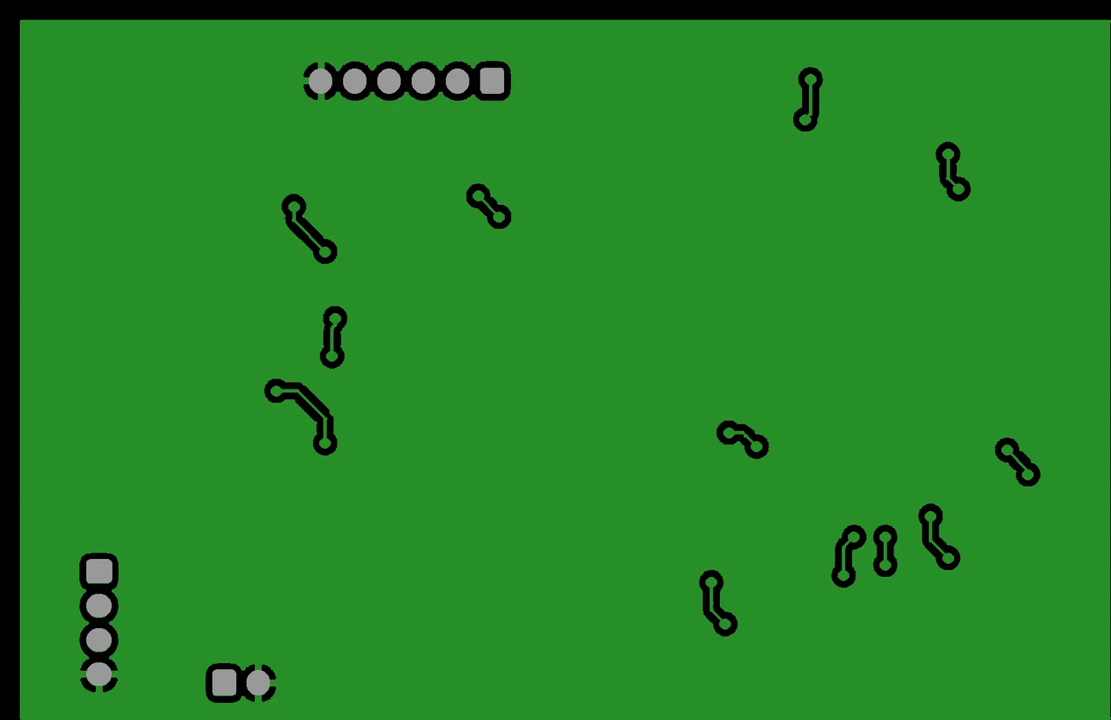
The KiCad project produced front/back copper, solder mask, paste, silkscreen, and edge cuts together with PTH/NPTH drills and a Gerber job file. Before sending the package to a manufacturer, the outline, layer polarity, apertures, and drill units still need a final CAM-viewer check.
Next validation
The current material covers circuitry, routing, and fabrication outputs. Board bring-up should begin with supply rails, clocks, SWD, and UART, followed by DC level and waveform checks on each PPG channel. Gain, cutoff, noise, SNR, and motion artifacts require measurement before sensor performance can be quantified. Automotive use would additionally require EMC, temperature, vibration, and long-term reliability testing.
Sources used
- STM32F411 PPG KiCad and Gerber archive — project-archive; circuit layout and fabrication-output review