Week 06
BJT Bias Design
I organize a study path from diodes to single-transistor amplifiers in the order that makes the circuit behavior easiest to revisit.
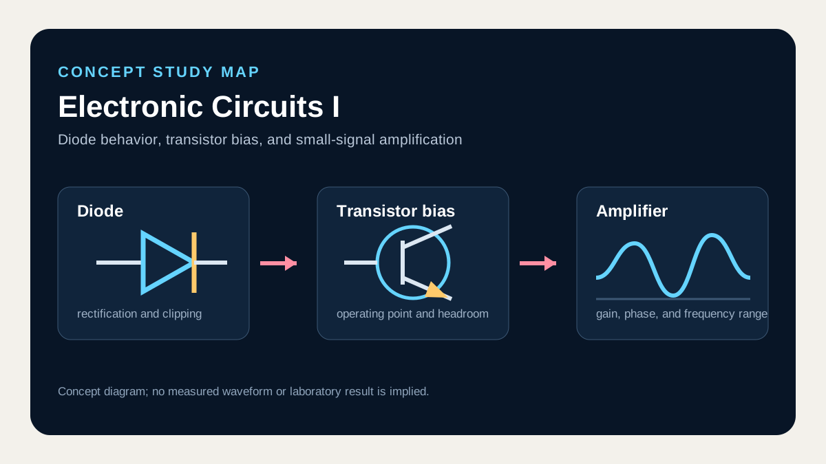
What I connect in this unit
Voltage-divider bias establishes the base voltage, and emitter degeneration feeds back an increase in current as an opposing emitter-voltage rise. Together they stabilize the quiescent point against beta and temperature variation while preserving signal swing.
Concept map
- Quiescent point
- Voltage-divider bias
- Emitter degeneration
- Thermal stability
Technical anchor
Replacing the divider by its Thevenin equivalent gives IB = (VTH − VBE)/(RTH + (β+1)RE) for the bias calculation.
How I review it
Evaluate IC and VCE at minimum and maximum beta, then check that the transistor remains forward active and leaves unclipped output swing at both extremes.
Connection to the full course
Unit 6 of 12. Unit numbers form a concept-study sequence and do not claim the original class schedule.