Week 01
Semiconductors and PN Junctions
I organize a study path from diodes to single-transistor amplifiers in the order that makes the circuit behavior easiest to revisit.
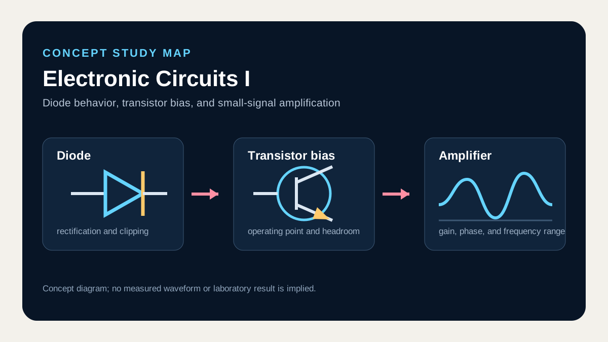
What I connect in this unit
Doping sets electron and hole concentrations in each semiconductor region. Joining p-type and n-type material causes diffusion, leaving a depletion region whose electric field establishes the built-in potential.
Concept map
- Electrons and holes
- Doping
- Depletion region
- Built-in potential
Technical anchor
At thermal equilibrium, Vbi = VT ln(NA·ND/ni²), so increasing the doping concentrations raises the built-in potential logarithmically.
How I review it
On an energy-band sketch, mark how depletion width and barrier height change under forward and reverse bias.
Connection to the full course
Unit 1 of 12. Unit numbers form a concept-study sequence and do not claim the original class schedule.