STM32 · Embedded · 03
F411 MCU, Power, and Pin Routing
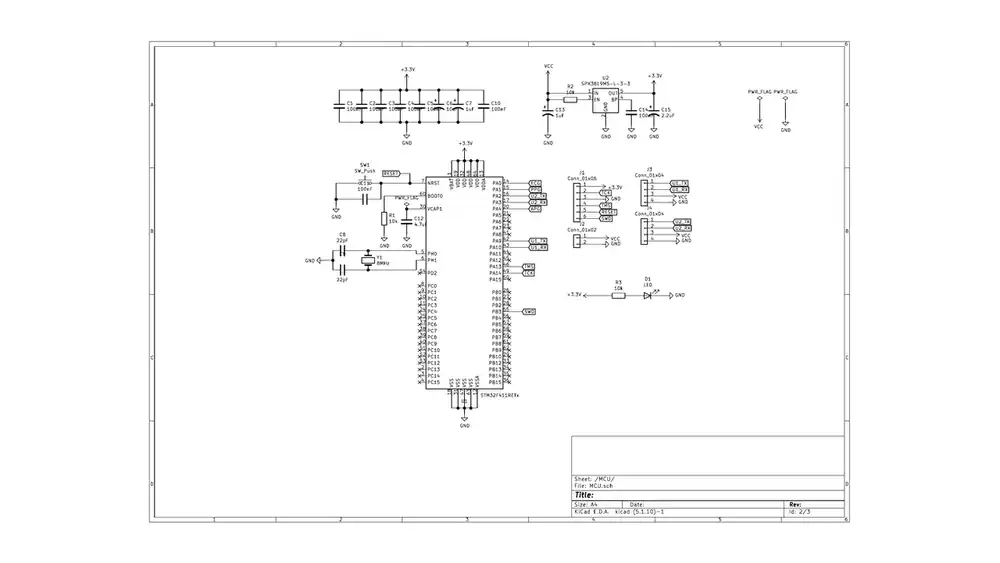
On the KiCad MCU sheet I checked the STM32F411RETx, 3.3 V rail, 8 MHz crystal, reset, SWD, and two UART paths. ECG enters PA0, PPG enters PA1, APG enters PA4, and USART2 uses PA2/PA3.
What I checked first
On the KiCad MCU sheet I checked the STM32F411RETx, 3.3 V rail, 8 MHz crystal, reset, SWD, and two UART paths. ECG enters PA0, PPG enters PA1, APG enters PA4, and USART2 uses PA2/PA3.
Source view
- I review VDDA/VSSA and digital-supply decoupling separately.
- RESET, BOOT0, SWDIO, and SWCLK define the programming and debug path.
- I cross-check schematic net labels against the CubeIDE pin assignment.
Implementation path
Only the saved configuration and processing sequence are shown.
Key terms
- STM32F411RETx
- 3.3 V
- ADC pins
- USART2
Review sequence
- STM32F411RETx
- 3.3 V → ADC pins
- USART2
Official references
- STM32CubeF4 Getting Started (UM1730)
- STM32 DSP with CMSIS (AN4841)
- Arm CMSIS-DSP
- STM32CubeF4 repository
The reviewed sources contain 22 prototype photos, a 40-slide STM setup deck, a three-page KiCad schematic, an ADC/UART note, an HRV module, two PPG code records, twelve top-level ECG C variants, and a complete CubeIDE project archive. I do not count byte-identical variants or ST/Arm vendor files as separate results, and I make no new performance claim without saved measurements.