Week 06
Boost Converters
I organize a study path from switching devices to converters and inverters while tracking power flow and device stress together.
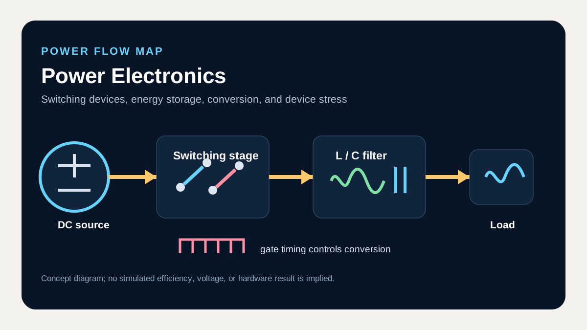
What I connect in this unit
A boost converter blocks the diode and stores energy in the inductor during switch on-time, then adds the input and inductor voltages to feed the capacitor and load during off-time. Volt-second balance across these states creates the step-up ratio, while output voltage sets the main diode and switch stress.
Concept map
- Step-up ratio
- Inductor charging
- Diode conduction
- Switch stress
Technical anchor
For ideal CCM operation, V_out = V_in/(1-D), and the on-interval ripple is Delta I_L = V_in D/(L f_s).
How I review it
Mark inductor-current direction on the on-state and off-state circuits, then verify switch voltage, diode reverse voltage, and inductor peak current together at maximum duty.
Connection to the full course
Unit 6 of 12. Unit numbers follow circuit dependencies and do not claim the original lecture schedule.