Week 02
Conduction and Switching Losses
I organize a study path from switching devices to converters and inverters while tracking power flow and device stress together.
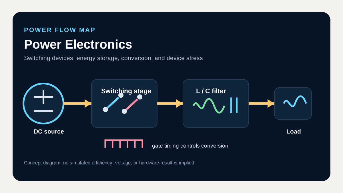
What I connect in this unit
On-state loss comes from the conducting voltage drop, whereas turn-on and turn-off losses arise from voltage-current overlap during transitions. Their sum becomes the heat source that raises junction temperature, so the electrical waveform and thermal-resistance network must be evaluated together.
Concept map
- On-state loss
- Turn-on loss
- Turn-off loss
- Junction temperature
Technical anchor
First-pass checks are P_cond = I_rms^2 R_DS(on) for a MOSFET, P_sw = f_s(E_on + E_off) for switching, and T_j = T_a + P_loss R_thetaJA for the thermal path.
How I review it
Use R_DS(on) or V_CE(sat) at the expected hot junction rather than the room-temperature headline value, then check margin across the heatsink, PCB, and ambient thermal path.
Connection to the full course
Unit 2 of 12. Unit numbers follow circuit dependencies and do not claim the original lecture schedule.