PADS · PCB Design · Schematic
Power, Measurement, and Communication Paths in a Multichannel Solar-Cell PCB
2026-09-04 · updated 2026-09-04 · Hyeongrok Ryu
Design analysis of power, ADC, DAC, and USB/UART paths across an STM32F401 mainboard and eight-channel measurement module.
- Series
- PADS PCB Design · 7
- Type / level
- project-log · advanced
- Tools
- PADS Logic, PADS Layout, STM32F401, AD7997, AD5629R, OPA703
Design purpose
Comparing several solar-cell channels under the same conditions requires per-channel current/voltage sensing, a setpoint path, shared power, and MCU communication. I traced each function through the STM32F401 mainboard and measurement-module files, focusing on where signals begin and which connector carries them.
STM32F401 mainboard
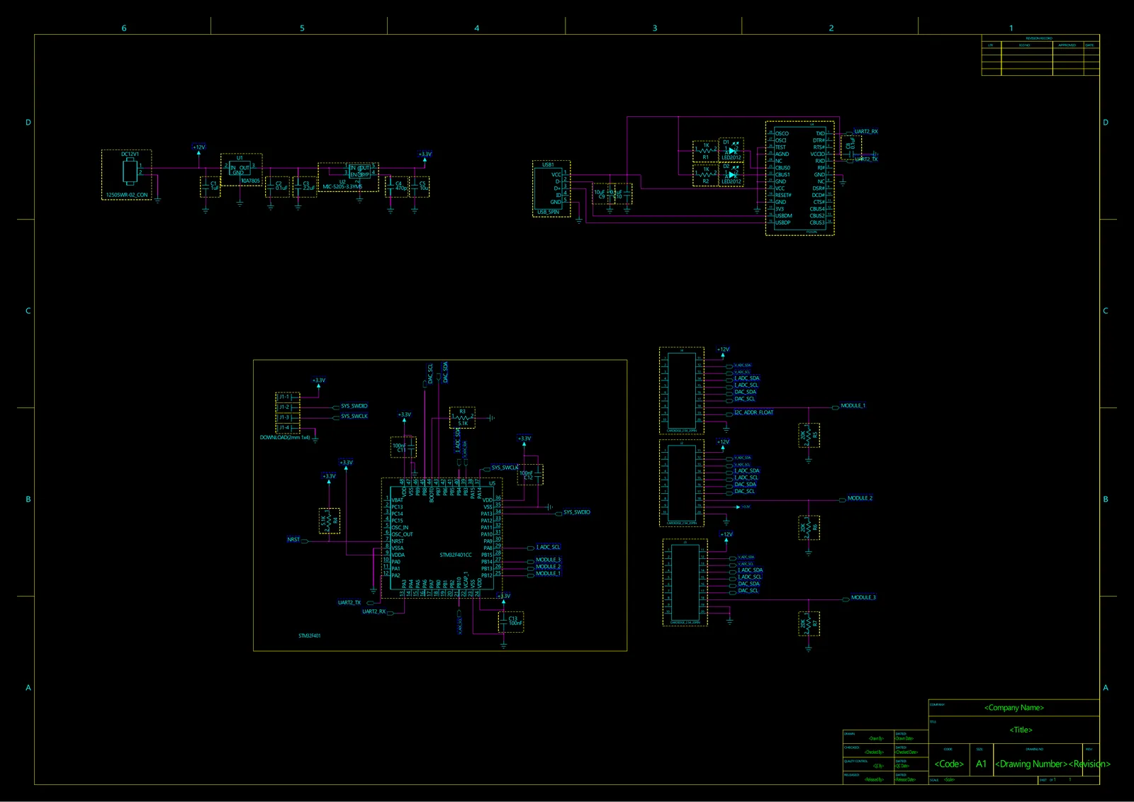
The 12-V input feeds 5-V and 3.3-V rails for the MCU and peripheral circuitry. The STM32F401 is accompanied by SWD, USB, and UART, while three connectors carry ADC/DAC buses, power, and address signals to measurement modules. Drawing the power tree before adding digital interfaces made power and communication faults easier to separate.
Eight-channel measurement module
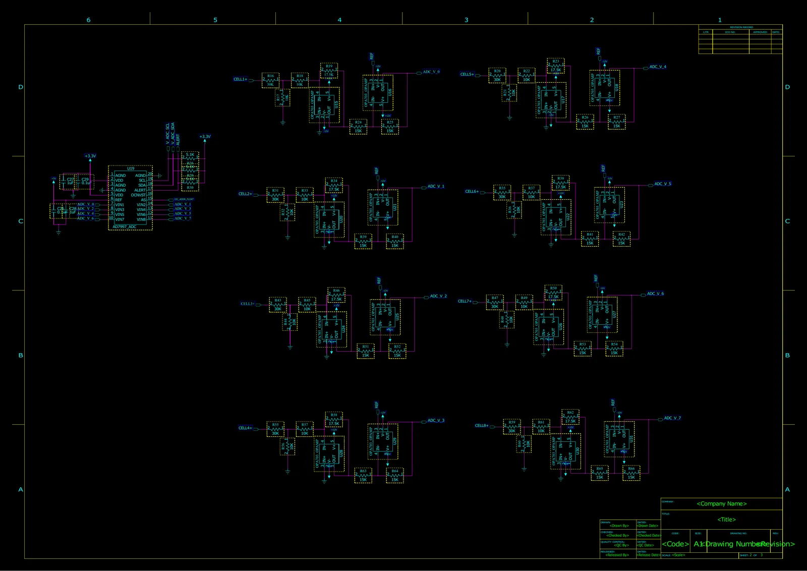
Eight current channels enter the module and an AD7997 ADC gathers them for the MCU. Another stored sheet contains OPA703 voltage paths and an AD5629R DAC, so measurement and actuation follow different signal chains. I read the circuit as input, conditioning, conversion, and communication rather than as a list of part numbers.
Control and data paths
The measurement direction runs from a cell channel through analog conditioning, ADC, MCU, and USB/UART. The control direction sends an MCU setpoint through the DAC to a channel-control path. Treating command and measurement separately makes missing nets easier to spot when comparing connector pins and names.
Measurement : Cell -> Analog path -> ADC -> MCU -> USB/UART
Control     : MCU setpoint -> DAC -> Channel control path
PCB and BOM artifacts
I compared the PADS schematics, PCB files, and parts list to match the major ICs and connectors. The public archive contains the STM32F401 mainboard and measurement-module schematic/PCB files plus the BOM. Installers, vendor PDFs, and temporary conversion products are excluded because they are not necessary to understand the design.
Attribution and next tests
The 12-channel MPPT concept references the 2021 IEEE PVSC paper by Kelzenberg, Loke, and Atwater. The paper and original-author Gerbers are linked rather than republished. Design files alone cannot establish accuracy, efficiency, temperature drift, or production yield. Before fabrication, current datasheets, reference voltage, and channel protection need a fresh review; calibration and load sweeps follow after assembly.
Sources used
- Solar-cell mainboard and measurement-module design archive — project-archive; circuit and PCB analysis
- Low-cost Open-source 12-channel MPPT Data Logger for Solar Cell Research — paper; 12-channel MPPT architecture reference