Electrical Engineering Coursework · High-Frequency Engineering
From a 3.5 GHz Microstrip to Wilkinson and Branch-Line Networks
2026-08-01 · updated 2026-08-01 · Hyeongrok Ryu
My review of alumina microstrip calculations and stored Cadence divider and hybrid screens.
- Series
- RF and Microwave · 3
- Type / level
- study-note · intermediate
- Tools
- Cadence Virtuoso, Smith Chart
Starting conditions
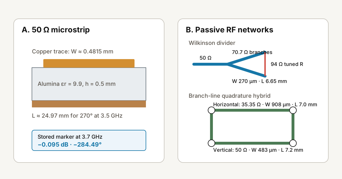
I began by collecting the shared assumptions from my RF coursework: a 0.5 mm alumina substrate, relative permittivity 9.9, and a 3.5 GHz design frequency. Those values set the microstrip width, guided wavelength, and quarter-wave sections used by both passive networks.
Width and length
The calculated width for a 50 Ω line was about 0.4815 mm. A 270° delay at 3.5 GHz is three quarters of the guided wavelength, giving a length near 24.97 mm. I initially confused the free-space wavelength with the shorter guided wavelength on alumina; separating them made the report value consistent.
| Item | Value | Use |
|---|---|---|
| Relative permittivity | 9.9 | Alumina |
| Substrate height | 0.5 mm | Shared condition |
| 50 Ω width | about 0.4815 mm | Microstrip calculation |
| 270° length | about 24.97 mm | at 3.5 GHz |
Reading the 3.7 GHz marker
A stored Cadence screen marks approximately −0.095 dB insertion loss and −284.49° phase at 3.7 GHz. The accumulated phase is larger than the 270° target at 3.5 GHz, which is consistent with observing the same line at a higher frequency. These are values read from the earlier simulation screen, not instrument measurements.
Wilkinson divider
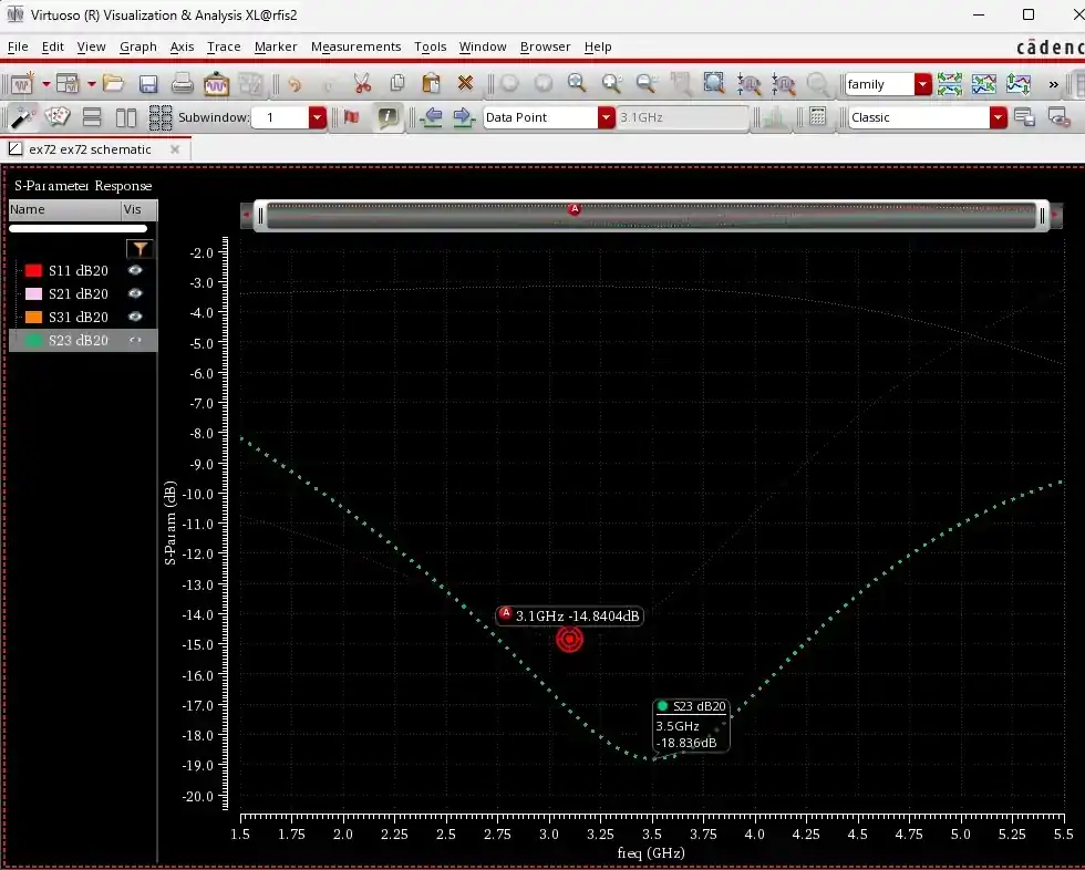
An equal-split Wilkinson uses two theoretical 70.7 Ω quarter-wave branches. The stored design tuned the resistor from 100 Ω to 94 Ω and used branch width 270 µm and length 6.65 mm. The screen places S21 and S31 near −3 dB and S11 near −15 dB. I treat the notch position and center-frequency alignment as items to check again instead of describing the match as perfect.
| Network | Transmission line | Reading from stored screen |
|---|---|---|
| Wilkinson | 70.7 Ω, W 270 µm, L 6.65 mm | S21/S31 near −3 dB, S11 near −15 dB |
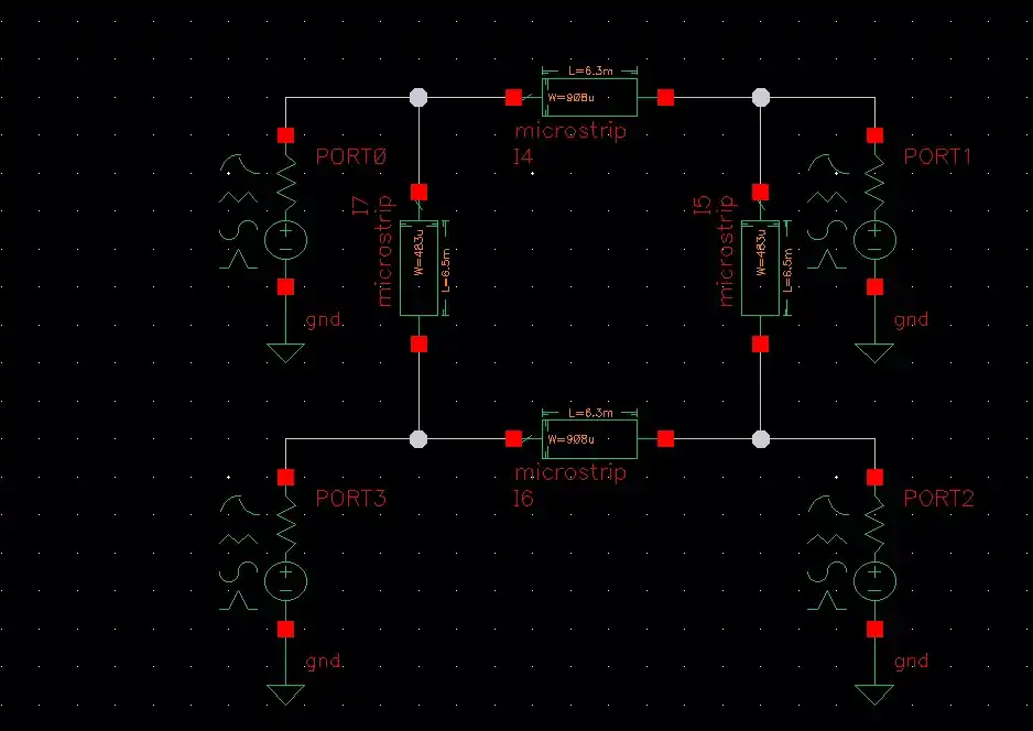
| Branch-line | 35.35 Ω horizontal, 50 Ω vertical | center shift in split and isolation curves |
Branch-line hybrid
The quadrature hybrid forms a rectangle with 35.35 Ω horizontal lines and 50 Ω vertical lines. The stored dimensions were W 908 µm and L 7.0 mm horizontally, then W 483 µm and L 7.2 mm vertically. Drawing the two widths separately helped me remember why the four sides do not share one impedance.
Simulation-only interpretation
Sources: report calculations and archived Cadence screens. Follow-up comparison conditions: matching frequency sweep, marker frequency, port definitions, and dB conventions. Fabricated-network VNA measurement is a separate experimental stage.
Previous and next
Sources used
- RF and Microwave coursework report and screenshots — local-coursework; dimensions and archived simulation markers