PADS · PCB Design · Decal and Footprint
Reading an SOIC Footprint and a PPG Schematic as Separate PADS Examples
2026-08-01 · updated 2026-08-01 · Hyeongrok Ryu
My notes on a six-pin SOIC decal and an OPA2333, filter, logic, and layout capture as two separate PADS examples.
- Series
- PADS PCB Design · 3
- Type / level
- study-note · intermediate
- Tools
- PADS Logic, PADS Layout
Why I kept the screens separate
I reopened a Decal Wizard capture and a separate PPG schematic/layout capture from the same study folder. Nothing in the saved material proves that the six-pin SOIC decal was used in the PPG design. I therefore placed them beside each other as two PADS exercises instead of inventing a shared part flow.
Six-pin SOIC dimensions
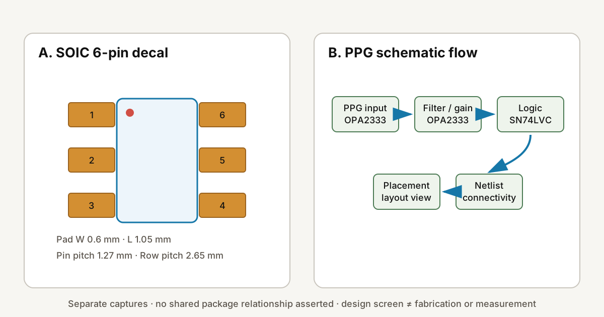
The Decal Wizard screen uses six SMD pins with pad width 0.6 mm and length 1.05 mm. Pin pitch is 1.27 mm along a row, while the distance between row centers is 2.65 mm. I initially mixed up lead span and row pitch, so I mapped each number back to a line on the package drawing.
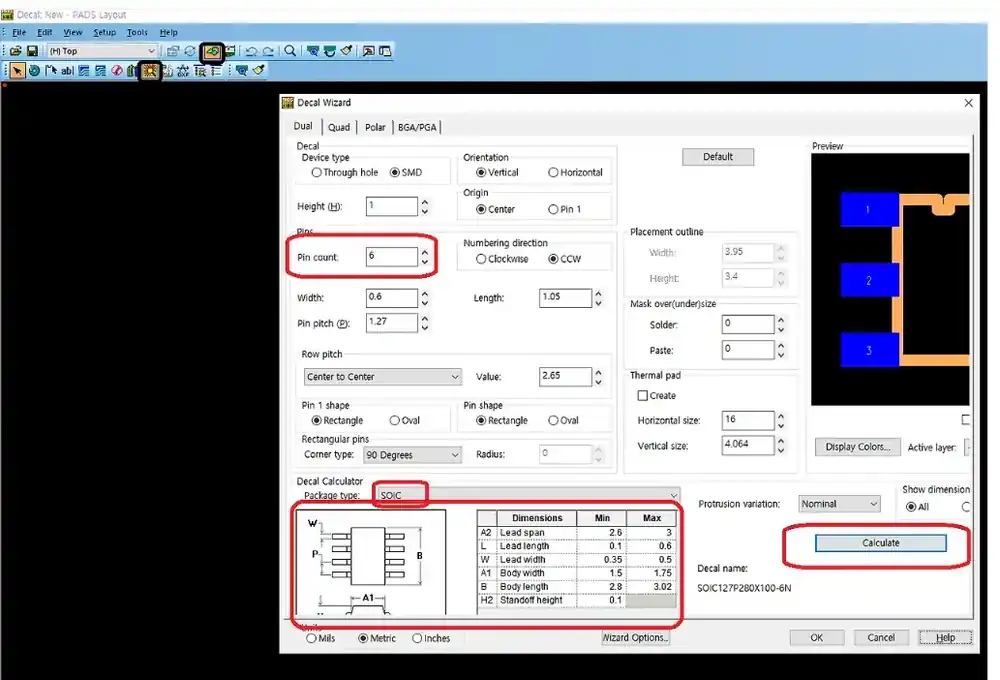
| Item | Entered value | Reference |
|---|---|---|
| Pin count | 6 | three on each side |
| Pad width | 0.6 mm | short pad dimension |
| Pad length | 1.05 mm | outward from body |
| Pin pitch | 1.27 mm | spacing within one row |
| Row pitch | 2.65 mm | distance between row centers |
Pin numbering and direction
The stored screen uses counter-clockwise numbering and a visible pin-1 mark. After building a footprint, I need to compare that numbering with the schematic symbol before checking anything else. A correct outline with the wrong pin map would still produce the wrong netlist.
PPG signal chain
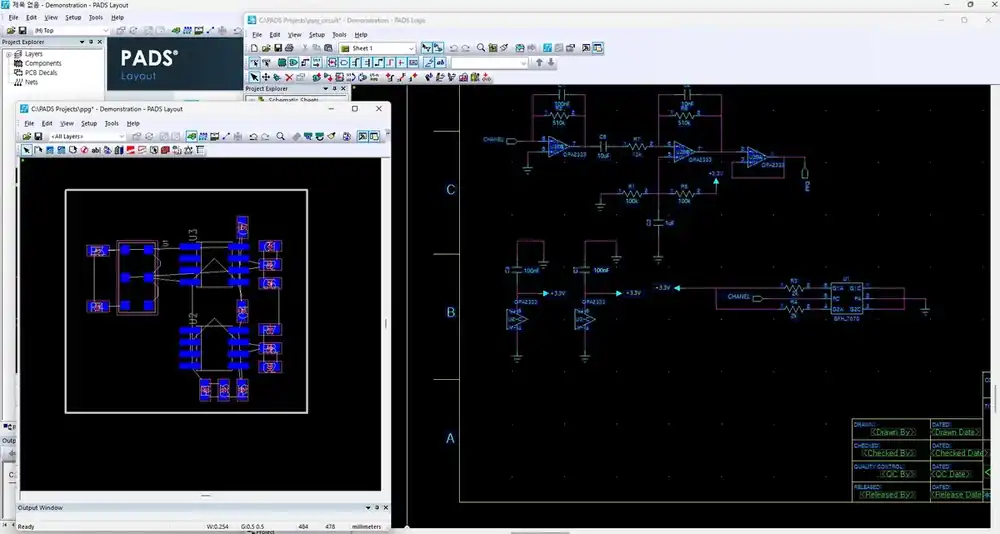
The separate PPG schematic screen shows OPA2333 amplification stages, RC filtering, and an SN74LVC-family logic stage. The signal is amplified and bandwidth-limited before it reaches the logic interface rather than being connected directly. I do not identify the visible OPA2333 package with the six-pin decal from the other capture.
PPG input
  → OPA2333 amplification
  → RC filtering and gain
  → OPA2333 output stage
  → SN74LVC logic interface
→ placement view in the PPG captureWhat the layout screen shows
The same capture places a PADS Logic schematic beside a PADS Layout placement view. It shows that parts and connectivity reached the layout stage. A design screen alone does not establish fabrication, completed DRC, or measured PPG performance.
My next check
Next I will compare the six-pin decal against its actual package drawing, including pin 1, pad dimensions, and courtyard. For the PPG design, I need a part-to-footprint mapping before inspecting packaging, net names, and unrouted connections. Until that mapping exists, I will keep the captures as separate artifacts.
Previous and next
Sources used
- PADS footprint and PPG design screenshots — local-coursework; two separate examples of decal dimensions and schematic-to-layout flow