<?xml version="1.0" encoding="utf-8"?><feed xmlns="http://www.w3.org/2005/Atom" xml:lang="ko"><generator uri="https://jekyllrb.com/" version="4.4.1">Jekyll</generator><link href="https://dororok9061.github.io/feed.xml" rel="self" type="application/atom+xml" /><link href="https://dororok9061.github.io/" rel="alternate" type="text/html" hreflang="ko" /><updated>2026-08-10T12:06:39+09:00</updated><id>https://dororok9061.github.io/feed.xml</id><title type="html">Hyeongrok Ryu Engineering Portfolio</title><subtitle>Hyeongrok Ryu&apos;s bilingual engineering portfolio for radar and embedded signal processing, FPGA RTL and digital verification, research, and publications.</subtitle><author><name>Hyeongrok Ryu</name><email>hnryu0515@gmail.com</email></author><entry xml:lang="en"><title type="html">PCB Research Publication Workbench public mirror</title><link href="https://dororok9061.github.io/en/blog/2026/08/08/pcb-research-portal-public-mirror/" rel="alternate" type="text/html" title="PCB Research Publication Workbench public mirror" /><published>2026-08-07T23:56:00+09:00</published><updated>2026-08-07T23:56:00+09:00</updated><id>https://dororok9061.github.io/en/blog/2026/08/08/pcb-research-portal-public-mirror-en</id><content type="html" xml:base="https://dororok9061.github.io/en/blog/2026/08/08/pcb-research-portal-public-mirror/"><![CDATA[<h2 id="mirror">Public mirror route</h2>

<p>The PCB inspection publication workbench that was checked on <code class="language-plaintext highlighter-rouge">127.0.0.1:8765</code> is now connected to the public GitHub Pages route again.</p>

<p><a href="/projects/pcb-visual-inspection/research-portal/?fresh=20260810-main-republish#methodology">Open the full Research Publication Workbench</a></p>

<p>The important change is that readers do not have to inspect one bundled contact sheet. The blog now exposes primary paper figures directly, while each card remains clickable through the site lightbox.</p>

<h2 id="key-figures">Key figures</h2>

<div class="publication-figure-grid">


<figure class="publication-figure-card">
  <button class="publication-figure-trigger" type="button" data-lightbox="/projects/pcb-visual-inspection/research-portal/AssetsWeb/paper_style/pcb_style_fig31a_capture_quality_gate.webp" data-lightbox-alt="Capture and quality gate" data-lightbox-caption="Capture and quality gate">
    <img class="publication-figure-image" src="/projects/pcb-visual-inspection/research-portal/AssetsWeb/paper_style/pcb_style_fig31a_capture_quality_gate.webp" alt="Capture and quality gate" width="900" height="900" loading="lazy" />
  </button>
  <figcaption class="publication-figure-caption">Capture and quality gate</figcaption>
</figure>


<figure class="publication-figure-card">
  <button class="publication-figure-trigger" type="button" data-lightbox="/projects/pcb-visual-inspection/research-portal/AssetsWeb/paper_style/pcb_style_fig31b_vit_dino_patch_path.webp" data-lightbox-alt="ViT DINO patch path" data-lightbox-caption="ViT DINO patch path">
    <img class="publication-figure-image" src="/projects/pcb-visual-inspection/research-portal/AssetsWeb/paper_style/pcb_style_fig31b_vit_dino_patch_path.webp" alt="ViT DINO patch path" width="900" height="900" loading="lazy" />
  </button>
  <figcaption class="publication-figure-caption">ViT DINO patch path</figcaption>
</figure>


<figure class="publication-figure-card">
  <button class="publication-figure-trigger" type="button" data-lightbox="/projects/pcb-visual-inspection/research-portal/AssetsWeb/paper_style/pcb_style_fig31c_registration_memory_bank.webp" data-lightbox-alt="Registration and memory bank" data-lightbox-caption="Registration and memory bank">
    <img class="publication-figure-image" src="/projects/pcb-visual-inspection/research-portal/AssetsWeb/paper_style/pcb_style_fig31c_registration_memory_bank.webp" alt="Registration and memory bank" width="900" height="900" loading="lazy" />
  </button>
  <figcaption class="publication-figure-caption">Registration and memory bank</figcaption>
</figure>


<figure class="publication-figure-card">
  <button class="publication-figure-trigger" type="button" data-lightbox="/projects/pcb-visual-inspection/research-portal/AssetsWeb/paper_style/pcb_style_fig13_heatmap_gt_mask.webp" data-lightbox-alt="Heatmap GT and mask" data-lightbox-caption="Heatmap GT and mask">
    <img class="publication-figure-image" src="/projects/pcb-visual-inspection/research-portal/AssetsWeb/paper_style/pcb_style_fig13_heatmap_gt_mask.webp" alt="Heatmap GT and mask" width="900" height="900" loading="lazy" />
  </button>
  <figcaption class="publication-figure-caption">Heatmap GT and mask</figcaption>
</figure>


<figure class="publication-figure-card">
  <button class="publication-figure-trigger" type="button" data-lightbox="/projects/pcb-visual-inspection/research-portal/AssetsWeb/paper_style/pcb_style_fig14_threshold_masks.webp" data-lightbox-alt="Threshold masks" data-lightbox-caption="Threshold masks">
    <img class="publication-figure-image" src="/projects/pcb-visual-inspection/research-portal/AssetsWeb/paper_style/pcb_style_fig14_threshold_masks.webp" alt="Threshold masks" width="900" height="900" loading="lazy" />
  </button>
  <figcaption class="publication-figure-caption">Threshold masks</figcaption>
</figure>


<figure class="publication-figure-card">
  <button class="publication-figure-trigger" type="button" data-lightbox="/projects/pcb-visual-inspection/research-portal/AssetsWeb/paper_style/pcb_style_fig15_dataset_examples.webp" data-lightbox-alt="Dataset examples" data-lightbox-caption="Dataset examples">
    <img class="publication-figure-image" src="/projects/pcb-visual-inspection/research-portal/AssetsWeb/paper_style/pcb_style_fig15_dataset_examples.webp" alt="Dataset examples" width="900" height="900" loading="lazy" />
  </button>
  <figcaption class="publication-figure-caption">Dataset examples</figcaption>
</figure>


<figure class="publication-figure-card">
  <button class="publication-figure-trigger" type="button" data-lightbox="/projects/pcb-visual-inspection/research-portal/AssetsWeb/paper_style/pcb_style_fig16_pro_line_chart.webp" data-lightbox-alt="Mean PRO line chart" data-lightbox-caption="Mean PRO line chart">
    <img class="publication-figure-image" src="/projects/pcb-visual-inspection/research-portal/AssetsWeb/paper_style/pcb_style_fig16_pro_line_chart.webp" alt="Mean PRO line chart" width="900" height="900" loading="lazy" />
  </button>
  <figcaption class="publication-figure-caption">Mean PRO line chart</figcaption>
</figure>


<figure class="publication-figure-card">
  <button class="publication-figure-trigger" type="button" data-lightbox="/projects/pcb-visual-inspection/research-portal/AssetsWeb/paper_style/pcb_style_fig18_loss_convergence.webp" data-lightbox-alt="Loss convergence" data-lightbox-caption="Loss convergence">
    <img class="publication-figure-image" src="/projects/pcb-visual-inspection/research-portal/AssetsWeb/paper_style/pcb_style_fig18_loss_convergence.webp" alt="Loss convergence" width="900" height="900" loading="lazy" />
  </button>
  <figcaption class="publication-figure-caption">Loss convergence</figcaption>
</figure>


<figure class="publication-figure-card">
  <button class="publication-figure-trigger" type="button" data-lightbox="/projects/pcb-visual-inspection/research-portal/AssetsWeb/paper_style/pcb_style_fig19_qualitative_grid.webp" data-lightbox-alt="Qualitative inspection grid" data-lightbox-caption="Qualitative inspection grid">
    <img class="publication-figure-image" src="/projects/pcb-visual-inspection/research-portal/AssetsWeb/paper_style/pcb_style_fig19_qualitative_grid.webp" alt="Qualitative inspection grid" width="900" height="900" loading="lazy" />
  </button>
  <figcaption class="publication-figure-caption">Qualitative inspection grid</figcaption>
</figure>


<figure class="publication-figure-card">
  <button class="publication-figure-trigger" type="button" data-lightbox="/projects/pcb-visual-inspection/research-portal/AssetsWeb/paper_style/pcb_style_fig25_embedding_filters.webp" data-lightbox-alt="Embedding filters" data-lightbox-caption="Embedding filters">
    <img class="publication-figure-image" src="/projects/pcb-visual-inspection/research-portal/AssetsWeb/paper_style/pcb_style_fig25_embedding_filters.webp" alt="Embedding filters" width="900" height="900" loading="lazy" />
  </button>
  <figcaption class="publication-figure-caption">Embedding filters</figcaption>
</figure>


<figure class="publication-figure-card">
  <button class="publication-figure-trigger" type="button" data-lightbox="/projects/pcb-visual-inspection/research-portal/AssetsWeb/paper_style/pcb_style_fig29_layer_attention_maps.webp" data-lightbox-alt="Layer attention maps" data-lightbox-caption="Layer attention maps">
    <img class="publication-figure-image" src="/projects/pcb-visual-inspection/research-portal/AssetsWeb/paper_style/pcb_style_fig29_layer_attention_maps.webp" alt="Layer attention maps" width="900" height="900" loading="lazy" />
  </button>
  <figcaption class="publication-figure-caption">Layer attention maps</figcaption>
</figure>


<figure class="publication-figure-card">
  <button class="publication-figure-trigger" type="button" data-lightbox="/projects/pcb-visual-inspection/research-portal/AssetsWeb/paper_style/pcb_style_table07_industrial_scores.webp" data-lightbox-alt="Industrial score tables" data-lightbox-caption="Industrial score tables">
    <img class="publication-figure-image" src="/projects/pcb-visual-inspection/research-portal/AssetsWeb/paper_style/pcb_style_table07_industrial_scores.webp" alt="Industrial score tables" width="900" height="900" loading="lazy" />
  </button>
  <figcaption class="publication-figure-caption">Industrial score tables</figcaption>
</figure>


<figure class="publication-figure-card">
  <button class="publication-figure-trigger" type="button" data-lightbox="/projects/pcb-visual-inspection/research-portal/AssetsWeb/paper_style/pcb_style_table09_full_result.webp" data-lightbox-alt="Full result table" data-lightbox-caption="Full result table">
    <img class="publication-figure-image" src="/projects/pcb-visual-inspection/research-portal/AssetsWeb/paper_style/pcb_style_table09_full_result.webp" alt="Full result table" width="900" height="900" loading="lazy" />
  </button>
  <figcaption class="publication-figure-caption">Full result table</figcaption>
</figure>

</div>

<h2 id="pipeline">Pipeline and architecture</h2>

<figure>
  <button type="button" data-lightbox="/projects/pcb-visual-inspection/research-portal/AssetsWeb/paper_style/pcb_style_fig09_frpatchcore_pipeline.webp" data-lightbox-alt="FR-PatchCore style PCB registration and memory-bank pipeline" data-lightbox-caption="FR-PatchCore style PCB registration and memory-bank pipeline">
    <img src="/projects/pcb-visual-inspection/research-portal/AssetsWeb/paper_style/pcb_style_fig09_frpatchcore_pipeline.webp" alt="FR-PatchCore style PCB registration and memory-bank pipeline" width="900" height="900" loading="lazy" />
  </button>
  <figcaption>The pipeline reconstructs registration, feature encoding, coreset memory bank, and kNN scoring for the PCB inspection setting.</figcaption>
</figure>

<figure>
  <button type="button" data-lightbox="/projects/pcb-visual-inspection/research-portal/AssetsWeb/paper_style/pcb_style_fig20_vit_model_overview.webp" data-lightbox-alt="ViT style PCB patch-token architecture" data-lightbox-caption="ViT style PCB patch-token architecture">
    <img src="/projects/pcb-visual-inspection/research-portal/AssetsWeb/paper_style/pcb_style_fig20_vit_model_overview.webp" alt="ViT style PCB patch-token architecture" width="900" height="900" loading="lazy" />
  </button>
  <figcaption>The architecture figure shows a PCB ROI converted into patch tokens and routed through a transformer encoder plus MLP head.</figcaption>
</figure>

<h2 id="results">Tables and claim boundary</h2>

<p>The public tables are registry-backed publication artifacts and research pilot evidence. They are not production acceptance claims. Live camera frame acquisition and gold-label production metrics remain gated until the supporting dataset is approved.</p>

<figure>
  <button type="button" data-lightbox="/projects/pcb-visual-inspection/research-portal/AssetsWeb/paper_style/pcb_style_table02_result_tables.webp" data-lightbox-alt="PCB result tables" data-lightbox-caption="PCB result tables">
    <img src="/projects/pcb-visual-inspection/research-portal/AssetsWeb/paper_style/pcb_style_table02_result_tables.webp" alt="PCB result tables" width="900" height="900" loading="lazy" />
  </button>
  <figcaption>The result table keeps the FR-PatchCore/PatchCore-style table layout while separating PCB inspection values from claim boundaries.</figcaption>
</figure>

<h2 id="links">Links</h2>

<ul>
  <li>GitHub repository: <a href="https://github.com/Dororok9061/PCB-Visual-Inspection-Studio">https://github.com/Dororok9061/PCB-Visual-Inspection-Studio</a></li>
  <li>Camera validation report: <a href="https://github.com/Dororok9061/PCB-Visual-Inspection-Studio/blob/main/docs/camera_validation_report.md">https://github.com/Dororok9061/PCB-Visual-Inspection-Studio/blob/main/docs/camera_validation_report.md</a></li>
  <li>Public research portal: <a href="https://dororok9061.github.io/projects/pcb-visual-inspection/research-portal/?fresh=20260810-main-republish#methodology">https://dororok9061.github.io/projects/pcb-visual-inspection/research-portal/?fresh=20260810-main-republish#methodology</a></li>
  <li>Korean version: <a href="/blog/2026/08/08/pcb-research-portal-public-mirror/?fresh=20260810-main-republish">PCB Research Publication Workbench 공개 미러</a></li>
</ul>]]></content><author><name>Hyeongrok Ryu</name></author><category term="pcb-inspection" /><category term="github-pages" /><category term="figure-atlas" /><category term="lightbox" /><summary type="html"><![CDATA[The PCB inspection figure atlas and lightbox flow verified on the local 8765 portal are now reflected in the GitHub Pages blog and project hub.]]></summary><media:thumbnail xmlns:media="http://search.yahoo.com/mrss/" url="https://dororok9061.github.io/assets/images/og.jpg" /><media:content medium="image" url="https://dororok9061.github.io/assets/images/og.jpg" xmlns:media="http://search.yahoo.com/mrss/" /></entry><entry xml:lang="ko"><title type="html">PCB Research Publication Workbench 공개 미러</title><link href="https://dororok9061.github.io/blog/2026/08/08/pcb-research-portal-public-mirror/" rel="alternate" type="text/html" title="PCB Research Publication Workbench 공개 미러" /><published>2026-08-07T23:55:00+09:00</published><updated>2026-08-07T23:55:00+09:00</updated><id>https://dororok9061.github.io/blog/2026/08/08/pcb-research-portal-public-mirror-ko</id><content type="html" xml:base="https://dororok9061.github.io/blog/2026/08/08/pcb-research-portal-public-mirror/"><![CDATA[<h2 id="mirror">공개 미러 경로</h2>

<p>로컬 <code class="language-plaintext highlighter-rouge">127.0.0.1:8765</code> 포털에서 확인하던 PCB inspection publication workbench를 GitHub Pages 경로로 다시 연결했습니다.</p>

<p><a href="/projects/pcb-visual-inspection/research-portal/?fresh=20260810-main-republish#methodology">전체 Research Publication Workbench 열기</a></p>

<p>이번 반영의 핵심은 contact sheet 하나로 뭉쳐 보이는 방식이 아니라, 논문 본문에서 바로 읽을 수 있는 대표 그림과 개별 확대 가능한 figure card를 함께 노출하는 것입니다. 각 그림은 <code class="language-plaintext highlighter-rouge">data-lightbox</code>를 통해 클릭하면 크게 볼 수 있습니다.</p>

<h2 id="key-figures">주요 그림</h2>

<div class="publication-figure-grid">


<figure class="publication-figure-card">
  <button class="publication-figure-trigger" type="button" data-lightbox="/projects/pcb-visual-inspection/research-portal/AssetsWeb/paper_style/pcb_style_fig31a_capture_quality_gate.webp" data-lightbox-alt="Capture and quality gate" data-lightbox-caption="Capture and quality gate">
    <img class="publication-figure-image" src="/projects/pcb-visual-inspection/research-portal/AssetsWeb/paper_style/pcb_style_fig31a_capture_quality_gate.webp" alt="Capture and quality gate" width="900" height="900" loading="lazy" />
  </button>
  <figcaption class="publication-figure-caption">Capture and quality gate</figcaption>
</figure>


<figure class="publication-figure-card">
  <button class="publication-figure-trigger" type="button" data-lightbox="/projects/pcb-visual-inspection/research-portal/AssetsWeb/paper_style/pcb_style_fig31b_vit_dino_patch_path.webp" data-lightbox-alt="ViT DINO patch path" data-lightbox-caption="ViT DINO patch path">
    <img class="publication-figure-image" src="/projects/pcb-visual-inspection/research-portal/AssetsWeb/paper_style/pcb_style_fig31b_vit_dino_patch_path.webp" alt="ViT DINO patch path" width="900" height="900" loading="lazy" />
  </button>
  <figcaption class="publication-figure-caption">ViT DINO patch path</figcaption>
</figure>


<figure class="publication-figure-card">
  <button class="publication-figure-trigger" type="button" data-lightbox="/projects/pcb-visual-inspection/research-portal/AssetsWeb/paper_style/pcb_style_fig31c_registration_memory_bank.webp" data-lightbox-alt="Registration and memory bank" data-lightbox-caption="Registration and memory bank">
    <img class="publication-figure-image" src="/projects/pcb-visual-inspection/research-portal/AssetsWeb/paper_style/pcb_style_fig31c_registration_memory_bank.webp" alt="Registration and memory bank" width="900" height="900" loading="lazy" />
  </button>
  <figcaption class="publication-figure-caption">Registration and memory bank</figcaption>
</figure>


<figure class="publication-figure-card">
  <button class="publication-figure-trigger" type="button" data-lightbox="/projects/pcb-visual-inspection/research-portal/AssetsWeb/paper_style/pcb_style_fig13_heatmap_gt_mask.webp" data-lightbox-alt="Heatmap GT and mask" data-lightbox-caption="Heatmap GT and mask">
    <img class="publication-figure-image" src="/projects/pcb-visual-inspection/research-portal/AssetsWeb/paper_style/pcb_style_fig13_heatmap_gt_mask.webp" alt="Heatmap GT and mask" width="900" height="900" loading="lazy" />
  </button>
  <figcaption class="publication-figure-caption">Heatmap GT and mask</figcaption>
</figure>


<figure class="publication-figure-card">
  <button class="publication-figure-trigger" type="button" data-lightbox="/projects/pcb-visual-inspection/research-portal/AssetsWeb/paper_style/pcb_style_fig14_threshold_masks.webp" data-lightbox-alt="Threshold masks" data-lightbox-caption="Threshold masks">
    <img class="publication-figure-image" src="/projects/pcb-visual-inspection/research-portal/AssetsWeb/paper_style/pcb_style_fig14_threshold_masks.webp" alt="Threshold masks" width="900" height="900" loading="lazy" />
  </button>
  <figcaption class="publication-figure-caption">Threshold masks</figcaption>
</figure>


<figure class="publication-figure-card">
  <button class="publication-figure-trigger" type="button" data-lightbox="/projects/pcb-visual-inspection/research-portal/AssetsWeb/paper_style/pcb_style_fig15_dataset_examples.webp" data-lightbox-alt="Dataset examples" data-lightbox-caption="Dataset examples">
    <img class="publication-figure-image" src="/projects/pcb-visual-inspection/research-portal/AssetsWeb/paper_style/pcb_style_fig15_dataset_examples.webp" alt="Dataset examples" width="900" height="900" loading="lazy" />
  </button>
  <figcaption class="publication-figure-caption">Dataset examples</figcaption>
</figure>


<figure class="publication-figure-card">
  <button class="publication-figure-trigger" type="button" data-lightbox="/projects/pcb-visual-inspection/research-portal/AssetsWeb/paper_style/pcb_style_fig16_pro_line_chart.webp" data-lightbox-alt="Mean PRO line chart" data-lightbox-caption="Mean PRO line chart">
    <img class="publication-figure-image" src="/projects/pcb-visual-inspection/research-portal/AssetsWeb/paper_style/pcb_style_fig16_pro_line_chart.webp" alt="Mean PRO line chart" width="900" height="900" loading="lazy" />
  </button>
  <figcaption class="publication-figure-caption">Mean PRO line chart</figcaption>
</figure>


<figure class="publication-figure-card">
  <button class="publication-figure-trigger" type="button" data-lightbox="/projects/pcb-visual-inspection/research-portal/AssetsWeb/paper_style/pcb_style_fig18_loss_convergence.webp" data-lightbox-alt="Loss convergence" data-lightbox-caption="Loss convergence">
    <img class="publication-figure-image" src="/projects/pcb-visual-inspection/research-portal/AssetsWeb/paper_style/pcb_style_fig18_loss_convergence.webp" alt="Loss convergence" width="900" height="900" loading="lazy" />
  </button>
  <figcaption class="publication-figure-caption">Loss convergence</figcaption>
</figure>


<figure class="publication-figure-card">
  <button class="publication-figure-trigger" type="button" data-lightbox="/projects/pcb-visual-inspection/research-portal/AssetsWeb/paper_style/pcb_style_fig19_qualitative_grid.webp" data-lightbox-alt="Qualitative inspection grid" data-lightbox-caption="Qualitative inspection grid">
    <img class="publication-figure-image" src="/projects/pcb-visual-inspection/research-portal/AssetsWeb/paper_style/pcb_style_fig19_qualitative_grid.webp" alt="Qualitative inspection grid" width="900" height="900" loading="lazy" />
  </button>
  <figcaption class="publication-figure-caption">Qualitative inspection grid</figcaption>
</figure>


<figure class="publication-figure-card">
  <button class="publication-figure-trigger" type="button" data-lightbox="/projects/pcb-visual-inspection/research-portal/AssetsWeb/paper_style/pcb_style_fig25_embedding_filters.webp" data-lightbox-alt="Embedding filters" data-lightbox-caption="Embedding filters">
    <img class="publication-figure-image" src="/projects/pcb-visual-inspection/research-portal/AssetsWeb/paper_style/pcb_style_fig25_embedding_filters.webp" alt="Embedding filters" width="900" height="900" loading="lazy" />
  </button>
  <figcaption class="publication-figure-caption">Embedding filters</figcaption>
</figure>


<figure class="publication-figure-card">
  <button class="publication-figure-trigger" type="button" data-lightbox="/projects/pcb-visual-inspection/research-portal/AssetsWeb/paper_style/pcb_style_fig29_layer_attention_maps.webp" data-lightbox-alt="Layer attention maps" data-lightbox-caption="Layer attention maps">
    <img class="publication-figure-image" src="/projects/pcb-visual-inspection/research-portal/AssetsWeb/paper_style/pcb_style_fig29_layer_attention_maps.webp" alt="Layer attention maps" width="900" height="900" loading="lazy" />
  </button>
  <figcaption class="publication-figure-caption">Layer attention maps</figcaption>
</figure>


<figure class="publication-figure-card">
  <button class="publication-figure-trigger" type="button" data-lightbox="/projects/pcb-visual-inspection/research-portal/AssetsWeb/paper_style/pcb_style_table07_industrial_scores.webp" data-lightbox-alt="Industrial score tables" data-lightbox-caption="Industrial score tables">
    <img class="publication-figure-image" src="/projects/pcb-visual-inspection/research-portal/AssetsWeb/paper_style/pcb_style_table07_industrial_scores.webp" alt="Industrial score tables" width="900" height="900" loading="lazy" />
  </button>
  <figcaption class="publication-figure-caption">Industrial score tables</figcaption>
</figure>


<figure class="publication-figure-card">
  <button class="publication-figure-trigger" type="button" data-lightbox="/projects/pcb-visual-inspection/research-portal/AssetsWeb/paper_style/pcb_style_table09_full_result.webp" data-lightbox-alt="Full result table" data-lightbox-caption="Full result table">
    <img class="publication-figure-image" src="/projects/pcb-visual-inspection/research-portal/AssetsWeb/paper_style/pcb_style_table09_full_result.webp" alt="Full result table" width="900" height="900" loading="lazy" />
  </button>
  <figcaption class="publication-figure-caption">Full result table</figcaption>
</figure>

</div>

<h2 id="pipeline">파이프라인과 아키텍처</h2>

<figure>
  <button type="button" data-lightbox="/projects/pcb-visual-inspection/research-portal/AssetsWeb/paper_style/pcb_style_fig09_frpatchcore_pipeline.webp" data-lightbox-alt="FR-PatchCore style PCB registration and memory-bank pipeline" data-lightbox-caption="FR-PatchCore style PCB registration and memory-bank pipeline">
    <img src="/projects/pcb-visual-inspection/research-portal/AssetsWeb/paper_style/pcb_style_fig09_frpatchcore_pipeline.webp" alt="FR-PatchCore style PCB registration and memory-bank pipeline" width="900" height="900" loading="lazy" />
  </button>
  <figcaption>등록, feature encoding, coreset memory bank, kNN score 흐름을 PCB inspection 데이터에 맞춰 재구성한 파이프라인입니다.</figcaption>
</figure>

<figure>
  <button type="button" data-lightbox="/projects/pcb-visual-inspection/research-portal/AssetsWeb/paper_style/pcb_style_fig20_vit_model_overview.webp" data-lightbox-alt="ViT style PCB patch-token architecture" data-lightbox-caption="ViT style PCB patch-token architecture">
    <img src="/projects/pcb-visual-inspection/research-portal/AssetsWeb/paper_style/pcb_style_fig20_vit_model_overview.webp" alt="ViT style PCB patch-token architecture" width="900" height="900" loading="lazy" />
  </button>
  <figcaption>PCB ROI를 patch token으로 바꾸고, transformer encoder와 MLP head로 연결하는 논문형 아키텍처 그림입니다.</figcaption>
</figure>

<h2 id="results">결과표와 주장 경계</h2>

<p>공개 페이지의 표와 수치는 production acceptance가 아니라, 출판 패키지와 연구용 pilot evidence를 설명하기 위한 registry-backed 결과입니다. 실물 카메라 프레임 수신과 gold-label production 성능은 아직 별도 승인 전입니다.</p>

<figure>
  <button type="button" data-lightbox="/projects/pcb-visual-inspection/research-portal/AssetsWeb/paper_style/pcb_style_table02_result_tables.webp" data-lightbox-alt="PCB result tables" data-lightbox-caption="PCB result tables">
    <img src="/projects/pcb-visual-inspection/research-portal/AssetsWeb/paper_style/pcb_style_table02_result_tables.webp" alt="PCB result tables" width="900" height="900" loading="lazy" />
  </button>
  <figcaption>FR-PatchCore/PatchCore-style table format을 유지하면서 PCB inspection 수치와 claim boundary를 분리한 결과표입니다.</figcaption>
</figure>

<h2 id="links">연결 경로</h2>

<ul>
  <li>GitHub repository: <a href="https://github.com/Dororok9061/PCB-Visual-Inspection-Studio">https://github.com/Dororok9061/PCB-Visual-Inspection-Studio</a></li>
  <li>Camera validation report: <a href="https://github.com/Dororok9061/PCB-Visual-Inspection-Studio/blob/main/docs/camera_validation_report.md">https://github.com/Dororok9061/PCB-Visual-Inspection-Studio/blob/main/docs/camera_validation_report.md</a></li>
  <li>Public research portal: <a href="https://dororok9061.github.io/projects/pcb-visual-inspection/research-portal/?fresh=20260810-main-republish#methodology">https://dororok9061.github.io/projects/pcb-visual-inspection/research-portal/?fresh=20260810-main-republish#methodology</a></li>
  <li>English version: <a href="/en/blog/2026/08/08/pcb-research-portal-public-mirror/?fresh=20260810-main-republish">PCB Research Publication Workbench public mirror</a></li>
</ul>]]></content><author><name>Hyeongrok Ryu</name></author><category term="pcb-inspection" /><category term="github-pages" /><category term="figure-atlas" /><category term="lightbox" /><summary type="html"><![CDATA[로컬 8765 포털에서 검증한 PCB inspection figure atlas와 lightbox 구성을 GitHub Pages 블로그와 프로젝트 허브에 다시 반영했습니다.]]></summary><media:thumbnail xmlns:media="http://search.yahoo.com/mrss/" url="https://dororok9061.github.io/assets/images/og.jpg" /><media:content medium="image" url="https://dororok9061.github.io/assets/images/og.jpg" xmlns:media="http://search.yahoo.com/mrss/" /></entry><entry xml:lang="en"><title type="html">Cascaded PI Control and Field Weakening for a DC Motor in PSIM</title><link href="https://dororok9061.github.io/en/blog/2026/08/01/dc-motor-cascaded-pi-field-weakening/" rel="alternate" type="text/html" title="Cascaded PI Control and Field Weakening for a DC Motor in PSIM" /><published>2026-08-01T15:20:00+09:00</published><updated>2026-08-01T15:20:00+09:00</updated><id>https://dororok9061.github.io/en/blog/2026/08/01/dc-motor-cascaded-pi-field-weakening-en</id><content type="html" xml:base="https://dororok9061.github.io/en/blog/2026/08/01/dc-motor-cascaded-pi-field-weakening/"><![CDATA[<h2 id="plant">Start with the motor and H-bridge</h2>

<p>I first reread the DC motor as coupled electrical and mechanical systems. The armature resistance and inductance sit with back EMF on the electrical side, while inertia, friction, and load torque form the mechanical side. The H-bridge supplies positive or negative average voltage to this plant. I start with a fixed-field operating point, where <code class="language-plaintext highlighter-rouge">K_e</code> and <code class="language-plaintext highlighter-rouge">K_t</code> can be treated as constants.</p>

<p class="study-equation"><code>vₐ = Rₐiₐ + Lₐ(diₐ/dt) + Kₑω</code><br /><code>J(dω/dt) = Kₜiₐ − Bω − Tₗ</code></p>

<p>Current creates torque, and speed feeds back through back EMF. This coupling explains why I should regulate current before asking the slower speed loop to command the plant.</p>

<h2 id="loops">Why I separated two loops</h2>

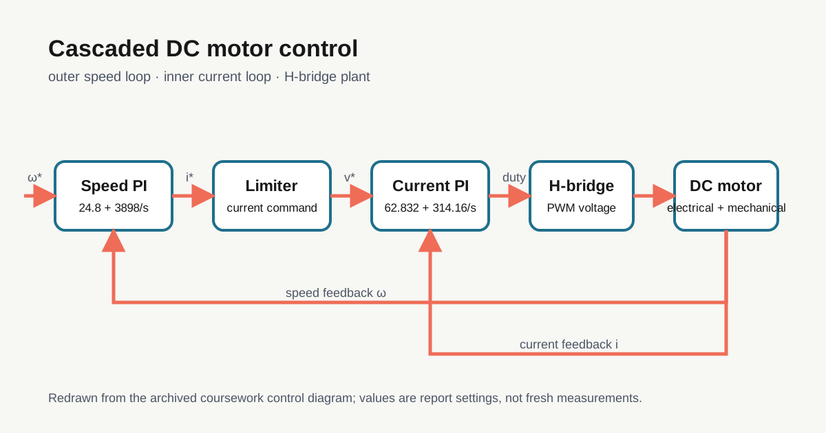
<p>The outer speed PI turns speed error into a current reference. The inner current PI tracks that reference and produces a voltage or duty command. With a faster current loop, the speed loop can treat the inner path approximately as a responsive torque source.</p>

<figure><img src="/assets/images/coursework/dc-motor-cascaded-control.svg" alt="Cascaded speed PI, current limiter, current PI, H-bridge, and DC motor" width="1200" height="630" /><figcaption>I redrew the block flow from the coursework report. The numbers are saved report settings, not fresh measurements.</figcaption></figure>

<p>I initially mixed up the two error signals. Writing units beside each block made the roles clear: the speed controller outputs current, while the current controller outputs voltage or duty.</p>

<h2 id="gains">Reading the saved PI settings</h2>

<p>The archived report records <code class="language-plaintext highlighter-rouge">Kp = 24.8</code>, <code class="language-plaintext highlighter-rouge">Ki ≈ 3898</code> for the speed PI and <code class="language-plaintext highlighter-rouge">Kp = 62.832</code>, <code class="language-plaintext highlighter-rouge">Ki = 314.16</code> for the current PI. I treat these as settings tied to that motor model and target bandwidth, not universal optimal gains.</p>

<div class="language-text highlighter-rouge"><div class="highlight"><pre class="highlight"><code>1. Check every motor parameter and unit.
2. Close and test the current loop first.
3. Confirm the current limiter.
4. Close the speed loop afterward.
5. Record saturation and anti-windup behavior.
</code></pre></div></div>

<h2 id="weakening">Saturation and field weakening</h2>

<p>Back EMF grows with speed. Eventually the DC bus cannot provide more voltage to maintain the requested current. In the separately excited DC motor used by the assignment, field weakening increases resistance in the field-current path, reducing field current and flux <code class="language-plaintext highlighter-rouge">Φ</code>.</p>

<p class="study-equation"><code>Kₑ = kₑΦ, Kₜ = kₜΦ</code></p>

<p>Reducing flux lowers back EMF at a given speed and leaves room to run faster, but armature current must rise to preserve the same torque. The constant-<code class="language-plaintext highlighter-rouge">K_e</code>, constant-<code class="language-plaintext highlighter-rouge">K_t</code> model from the first section therefore does not apply unchanged in this region. I use Altair’s PSIM material only as general context for nested loops and operation above base speed; the archived assignment report is the source for this DC field-circuit implementation.</p>

<h2 id="ripple">Switching-frequency comparison</h2>

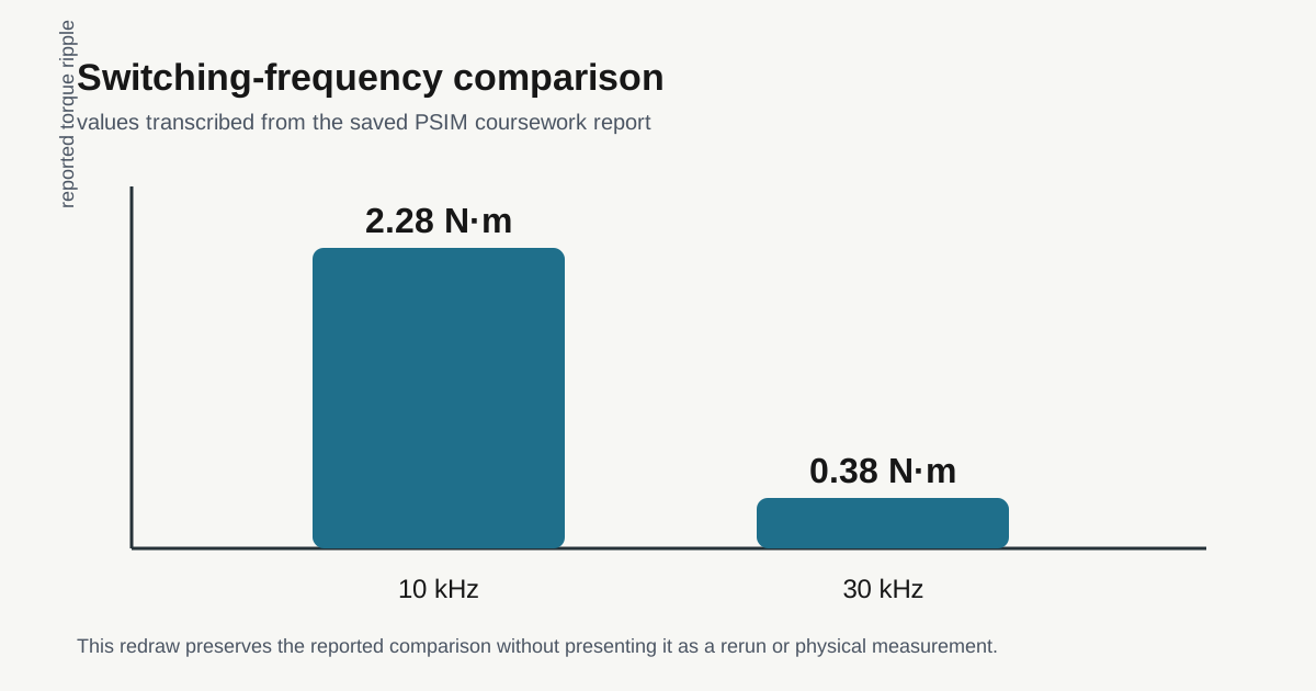
<p>The report records 2.28 N·m of torque ripple at 10 kHz and 0.38 N·m at 30 kHz. These are saved PSIM simulation values, not measurements from a physical shaft.</p>

<figure><img src="/assets/images/coursework/dc-motor-switching-ripple.svg" alt="Saved torque-ripple comparison of 2.28 newton metres at 10 kilohertz and 0.38 newton metres at 30 kilohertz" width="1200" height="630" /><figcaption>I placed the two archived values on one scale. The comparison supports lower simulated ripple, not a claim about loss, temperature, or EMI.</figcaption></figure>

<p>A higher switching frequency can reduce the current change per switching period, but it can also increase switching loss, EMI, and computation demand. I therefore keep this as a one-metric simulation comparison.</p>

<h2 id="limits">Scope of this note</h2>

<p>I have reread the archived model, gains, and plots and redrawn the control structure. I have not rerun the original PSIM circuit in a current environment or connected a physical motor. My next step is to rerun the inner-loop step response first and compare saturation with and without anti-windup under identical conditions.</p>]]></content><author><name>Hyeongrok Ryu</name></author><category term="dc-motor" /><category term="psim" /><category term="pi-control" /><category term="h-bridge" /><category term="field-weakening" /><summary type="html"><![CDATA[My study note on the H-bridge, nested current and speed loops, and switching-frequency comparison in an archived motor-control report.]]></summary><media:thumbnail xmlns:media="http://search.yahoo.com/mrss/" url="https://dororok9061.github.io/assets/images/og.jpg" /><media:content medium="image" url="https://dororok9061.github.io/assets/images/og.jpg" xmlns:media="http://search.yahoo.com/mrss/" /></entry><entry xml:lang="ko"><title type="html">PSIM에서 DC Motor 이중 PI 제어와 Field Weakening 정리</title><link href="https://dororok9061.github.io/blog/2026/08/01/dc-motor-cascaded-pi-field-weakening/" rel="alternate" type="text/html" title="PSIM에서 DC Motor 이중 PI 제어와 Field Weakening 정리" /><published>2026-08-01T15:20:00+09:00</published><updated>2026-08-01T15:20:00+09:00</updated><id>https://dororok9061.github.io/blog/2026/08/01/dc-motor-cascaded-pi-field-weakening-ko</id><content type="html" xml:base="https://dororok9061.github.io/blog/2026/08/01/dc-motor-cascaded-pi-field-weakening/"><![CDATA[<h2 id="plant">모터와 H-bridge부터 보기</h2>

<p>먼저 과제 보고서에서 DC Motor를 전기계와 기계계로 나눠 다시 읽었다. 전기계는 전기자 저항·인덕턴스와 역기전력으로, 기계계는 관성·마찰과 부하토크로 표현했다. H-bridge는 이 plant에 양·음의 평균 전압을 만들어 주는 구동부다.</p>

<p>전기자 회로는 먼저 자속이 일정한 기준 동작점으로 정리했다. 이때만 <code class="language-plaintext highlighter-rouge">K_e</code>와 <code class="language-plaintext highlighter-rouge">K_t</code>를 상수처럼 둘 수 있다.</p>

<p class="study-equation"><code>vₐ = Rₐiₐ + Lₐ(diₐ/dt) + Kₑω</code><br /><code>J(dω/dt) = Kₜiₐ − Bω − Tₗ</code></p>

<p>두 식을 같이 보면 전류가 토크를 만들고, 속도가 다시 역기전력으로 전류에 영향을 준다. 속도 명령만 바로 PWM에 연결하는 대신 전류를 안쪽에서 먼저 제어한 이유가 여기서 보였다.</p>

<h2 id="loops">두 제어루프를 나눈 이유</h2>

<p>바깥쪽 speed PI는 속도 오차를 전류 명령으로 바꾸고, 안쪽 current PI는 그 전류를 빠르게 추종하도록 전압 명령을 만든다. 전류루프의 대역폭을 속도루프보다 높게 잡으면 바깥쪽에서는 안쪽 루프를 거의 즉시 반응하는 토크원처럼 볼 수 있다.</p>

<figure><img src="/assets/images/coursework/dc-motor-cascaded-control.svg" alt="속도 PI, 전류 제한기, 전류 PI, H-bridge와 DC motor의 이중루프" width="1200" height="630" /><figcaption>과제 보고서의 블록도를 공개용으로 다시 그렸다. 수치는 당시 보고서에 적힌 설정이며 이번에 다시 실행한 값은 아니다.</figcaption></figure>

<p>처음에는 두 PI가 같은 오차를 줄이는 것으로 혼동했다. 다시 보니 speed PI의 출력은 전류 기준값이고, current PI의 출력은 전압 또는 duty 기준값이었다. 각 loop의 입력·출력 단위를 적어 두자 역할이 분명해졌다.</p>

<h2 id="gains">보고서의 PI 설정 읽기</h2>

<p>남아 있던 보고서에는 speed PI가 <code class="language-plaintext highlighter-rouge">Kp = 24.8</code>, <code class="language-plaintext highlighter-rouge">Ki ≈ 3898</code>, current PI가 <code class="language-plaintext highlighter-rouge">Kp = 62.832</code>, <code class="language-plaintext highlighter-rouge">Ki = 314.16</code>으로 기록돼 있었다. 이 값 자체를 보편적인 최적 gain으로 보지 않고, 보고서에서 사용한 motor parameter와 목표 대역폭에 종속된 설정으로 읽었다.</p>

<p>코드나 block parameter를 다시 확인할 때는 다음 순서가 안전하다.</p>

<div class="language-text highlighter-rouge"><div class="highlight"><pre class="highlight"><code>1. motor parameter와 단위를 확인한다.
2. current loop를 먼저 닫고 step response를 본다.
3. current limit가 동작하는지 확인한다.
4. 그 다음 speed loop를 닫는다.
5. saturation과 anti-windup 유무를 함께 기록한다.
</code></pre></div></div>

<h2 id="weakening">포화와 Field Weakening</h2>

<p>속도가 올라가면 역기전력 <code class="language-plaintext highlighter-rouge">K_e ω</code>도 커진다. DC bus가 만들 수 있는 전압을 다 써도 전류를 더 유지할 수 없는 영역에서는 전압 포화가 생긴다. 과제의 타여자 DC Motor에서는 계자회로 저항을 높여 계자전류와 자속 <code class="language-plaintext highlighter-rouge">Φ</code>를 줄이는 방식으로 field weakening을 구성했다.</p>

<p class="study-equation"><code>Kₑ = kₑΦ, Kₜ = kₜΦ</code></p>

<p>따라서 자속을 줄이면 같은 속도에서 역기전력은 낮아져 더 높은 속도로 갈 여지가 생기지만, 같은 토크를 내려면 전기자전류가 더 커져야 한다. 이 구간에서는 앞 절의 상수 <code class="language-plaintext highlighter-rouge">K_e</code>, <code class="language-plaintext highlighter-rouge">K_t</code> 가정을 그대로 쓸 수 없다. Altair의 PSIM 자료는 current·speed loop와 base-speed 이후 제어라는 일반 맥락만 비교하는 데 사용했고, 이 DC 계자회로 구현의 근거는 과제 보고서에서 읽었다.</p>

<h2 id="ripple">스위칭 주파수 비교</h2>

<p>과제 보고서에는 10 kHz에서 2.28 N·m, 30 kHz에서 0.38 N·m의 torque ripple이 기록돼 있었다. 이 값은 저장된 PSIM 시뮬레이션 비교이며, 실제 모터 샤프트에서 측정한 값이 아니다.</p>

<figure><img src="/assets/images/coursework/dc-motor-switching-ripple.svg" alt="10 kHz 2.28 뉴턴미터와 30 kHz 0.38 뉴턴미터의 저장된 torque ripple 비교" width="1200" height="630" /><figcaption>보고서에 적힌 두 결과를 같은 축으로 다시 그렸다. 높은 스위칭 주파수의 ripple 감소만 읽을 수 있고 손실·온도·EMI까지 좋아졌다고 말할 수는 없다.</figcaption></figure>

<p>주파수를 높이면 전류가 한 주기 동안 변할 시간이 짧아져 ripple이 줄 수 있다. 반면 switching loss와 EMI, 계산 부하는 커질 수 있다. 그래서 이번 비교는 ripple 하나의 시뮬레이션 결과로만 남겼다.</p>

<h2 id="limits">이번 기록의 범위</h2>

<p>이 단계까지는 저장된 과제 보고서의 모델, gain과 그래프를 다시 읽고 블록도를 재작성했다. PSIM 원본 회로를 새 버전에서 재실행하거나 실제 모터를 연결해 확인하지는 않았다. 다음에는 current-loop step부터 분리해 실행하고 saturation과 anti-windup 동작을 같은 조건에서 비교할 예정이다.</p>]]></content><author><name>Hyeongrok Ryu</name></author><category term="dc-motor" /><category term="psim" /><category term="pi-control" /><category term="h-bridge" /><category term="field-weakening" /><summary type="html"><![CDATA[전동기제어 과제 보고서의 H-bridge, 전류·속도 이중루프와 스위칭 주파수 비교를 다시 읽고 정리한 기록.]]></summary><media:thumbnail xmlns:media="http://search.yahoo.com/mrss/" url="https://dororok9061.github.io/assets/images/og.jpg" /><media:content medium="image" url="https://dororok9061.github.io/assets/images/og.jpg" xmlns:media="http://search.yahoo.com/mrss/" /></entry><entry xml:lang="en"><title type="html">Reading an SOIC Footprint and a PPG Schematic as Separate PADS Examples</title><link href="https://dororok9061.github.io/en/blog/2026/08/01/pads-footprint-ppg-schematic/" rel="alternate" type="text/html" title="Reading an SOIC Footprint and a PPG Schematic as Separate PADS Examples" /><published>2026-08-01T11:03:00+09:00</published><updated>2026-08-01T11:03:00+09:00</updated><id>https://dororok9061.github.io/en/blog/2026/08/01/pads-footprint-ppg-schematic-en</id><content type="html" xml:base="https://dororok9061.github.io/en/blog/2026/08/01/pads-footprint-ppg-schematic/"><![CDATA[<h2 id="start">Why I kept the screens separate</h2>

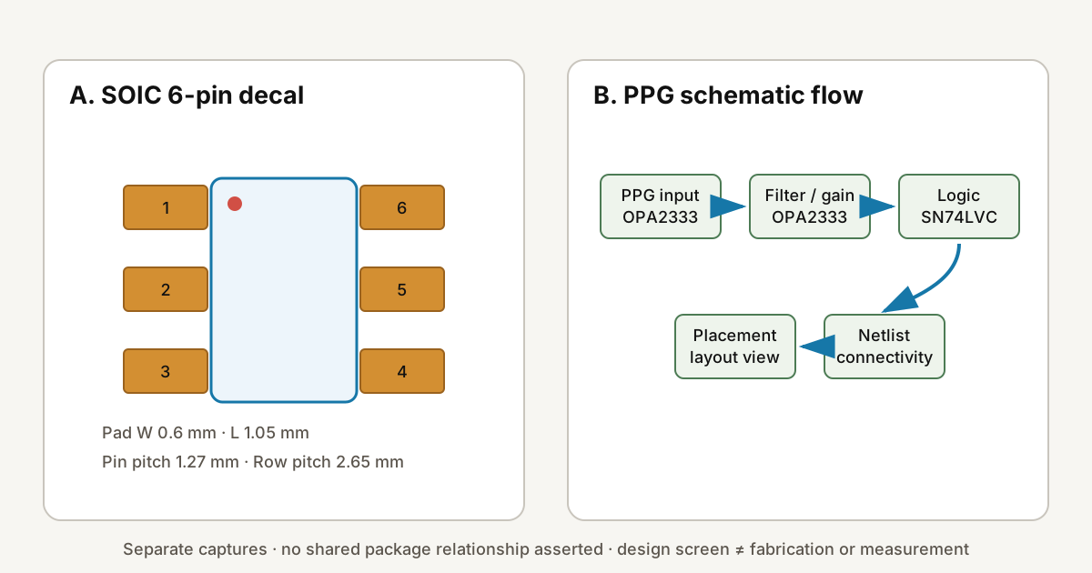
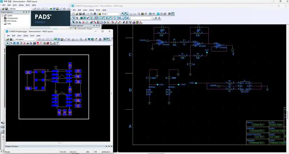
<p>I reopened a Decal Wizard capture and a separate PPG schematic/layout capture from the same study folder. Nothing in the saved material proves that the six-pin SOIC decal was used in the PPG design. I therefore placed them beside each other as two PADS exercises instead of inventing a shared part flow.</p>

<figure>
  <img src="/assets/images/learning/coursework/pads-footprint-ppg-schematic.svg" alt="An independent six-pad SOIC decal example beside a separate OPA2333, filter, SN74LVC logic, and layout example" width="1200" height="630" />
  <figcaption>The panels come from separate saved captures. Their placement does not imply that they share one package.</figcaption>
</figure>

<h2 id="footprint">Six-pin SOIC dimensions</h2>

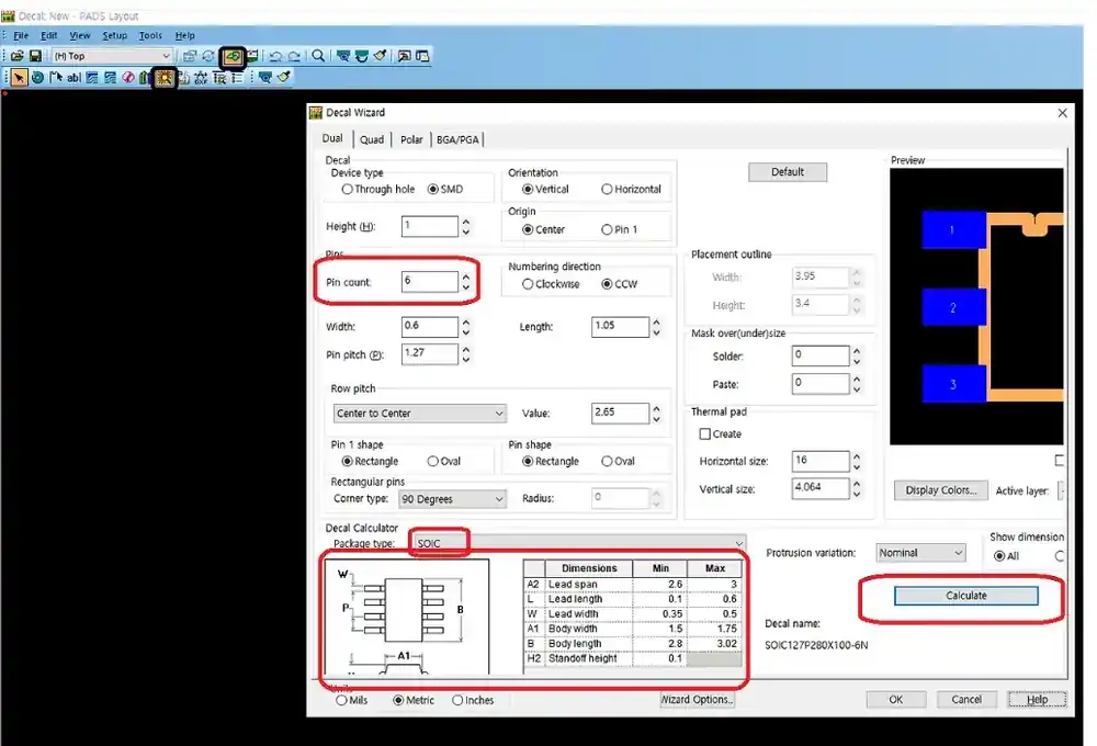
<p>The Decal Wizard screen uses six SMD pins with pad width 0.6 mm and length 1.05 mm. Pin pitch is 1.27 mm along a row, while the distance between row centers is 2.65 mm. I initially mixed up lead span and row pitch, so I mapped each number back to a line on the package drawing.</p>

<figure><img src="/assets/images/study/pads/pads-soic-decal-a.webp" alt="Saved PADS Decal Wizard screen with six-pin SOIC dimensions" width="1024" height="704" /><figcaption>I converted my saved Decal Wizard screen to WebP without metadata.</figcaption></figure>

<figure>
  <table>
    <thead><tr><th>Item</th><th>Entered value</th><th>Reference</th></tr></thead>
    <tbody>
      <tr><td>Pin count</td><td>6</td><td>three on each side</td></tr>
      <tr><td>Pad width</td><td>0.6 mm</td><td>short pad dimension</td></tr>
      <tr><td>Pad length</td><td>1.05 mm</td><td>outward from body</td></tr>
      <tr><td>Pin pitch</td><td>1.27 mm</td><td>spacing within one row</td></tr>
      <tr><td>Row pitch</td><td>2.65 mm</td><td>distance between row centers</td></tr>
    </tbody>
  </table>
  <figcaption>Pairing each number with its geometric reference made the wizard inputs less ambiguous.</figcaption>
</figure>

<h2 id="numbering">Pin numbering and direction</h2>

<p>The stored screen uses counter-clockwise numbering and a visible pin-1 mark. After building a footprint, I need to compare that numbering with the schematic symbol before checking anything else. A correct outline with the wrong pin map would still produce the wrong netlist.</p>

<h2 id="schematic">PPG signal chain</h2>

<p>The separate PPG schematic screen shows OPA2333 amplification stages, RC filtering, and an SN74LVC-family logic stage. The signal is amplified and bandwidth-limited before it reaches the logic interface rather than being connected directly. I do not identify the visible OPA2333 package with the six-pin decal from the other capture.</p>

<figure><img src="/assets/images/study/pads/pads-ppg-layout.webp" alt="Saved PADS screen with OPA2333 stages, SN74LVC logic, and early Layout placement" width="1904" height="1018" /><figcaption>This is the actual saved PADS schematic and early placement view.</figcaption></figure>

<figure>
  <pre><code>PPG input
  → OPA2333 amplification
  → RC filtering and gain
  → OPA2333 output stage
  → SN74LVC logic interface
  → placement view in the PPG capture</code></pre>
  <figcaption>I kept only the functional blocks visible in the saved screen and did not invent component values or cutoff frequencies.</figcaption>
</figure>

<h2 id="layout">What the layout screen shows</h2>

<p>The same capture places a PADS Logic schematic beside a PADS Layout placement view. It shows that parts and connectivity reached the layout stage. A design screen alone does not establish fabrication, completed DRC, or measured PPG performance.</p>

<h2 id="next">My next check</h2>

<p>Next I will compare the six-pin decal against its actual package drawing, including pin 1, pad dimensions, and courtyard. For the PPG design, I need a part-to-footprint mapping before inspecting packaging, net names, and unrouted connections. Until that mapping exists, I will keep the captures as separate artifacts.</p>

<h2 id="navigation">Previous and next</h2>

<ul>
  <li><a href="/en/coursework/">Previous: coursework overview</a></li>
  <li><a href="/en/blog/series/pads-pcb-design/">Series: PADS PCB Design</a></li>
  <li><a href="/en/projects/ppg-hrv/">Next: PPG-HRV project</a></li>
</ul>]]></content><author><name>Hyeongrok Ryu</name></author><category term="pads" /><category term="pcb-footprint" /><category term="ppg" /><category term="opa2333" /><summary type="html"><![CDATA[My notes on a six-pin SOIC decal and an OPA2333, filter, logic, and layout capture as two separate PADS examples.]]></summary><media:thumbnail xmlns:media="http://search.yahoo.com/mrss/" url="https://dororok9061.github.io/assets/images/og.jpg" /><media:content medium="image" url="https://dororok9061.github.io/assets/images/og.jpg" xmlns:media="http://search.yahoo.com/mrss/" /></entry><entry xml:lang="ko"><title type="html">PADS의 SOIC Footprint와 PPG 회로를 별도 사례로 다시 읽기</title><link href="https://dororok9061.github.io/blog/2026/08/01/pads-footprint-ppg-schematic/" rel="alternate" type="text/html" title="PADS의 SOIC Footprint와 PPG 회로를 별도 사례로 다시 읽기" /><published>2026-08-01T11:03:00+09:00</published><updated>2026-08-01T11:03:00+09:00</updated><id>https://dororok9061.github.io/blog/2026/08/01/pads-footprint-ppg-schematic-ko</id><content type="html" xml:base="https://dororok9061.github.io/blog/2026/08/01/pads-footprint-ppg-schematic/"><![CDATA[<h2 id="start">두 화면을 분리해서 본 이유</h2>

<p>PADS를 처음 배울 때 저장한 Decal Wizard 화면과 PPG schematic·layout 화면을 다시 펼쳐 봤다. 두 화면은 같은 폴더에 남아 있지만, 6-pin SOIC decal이 PPG 설계에 사용됐다고 확인할 연결 정보는 없었다. 그래서 하나의 부품 흐름으로 합치지 않고 footprint 입력과 schematic-to-layout 읽기를 서로 다른 사례로 나란히 정리했다.</p>

<figure>
  <img src="/assets/images/learning/coursework/pads-footprint-ppg-schematic.svg" alt="서로 독립된 사례로 배치한 여섯 pad SOIC decal과 OPA2333, filter, SN74LVC logic PPG 화면" width="1200" height="630" />
  <figcaption>왼쪽과 오른쪽은 별도 저장 화면에서 읽은 두 학습 사례다. 두 artifact가 같은 package를 공유한다고 뜻하지 않는다.</figcaption>
</figure>

<h2 id="footprint">6-pin SOIC 치수</h2>

<p>Decal Wizard 화면에서 pin count를 6으로 두고 SMD pad 폭 0.6 mm, 길이 1.05 mm를 입력했다. 같은 줄의 pin pitch는 1.27 mm, 양쪽 row 중심 간격은 2.65 mm였다. 처음에는 lead span과 row pitch를 같은 값으로 읽었는데, pad 중심을 기준으로 다시 보니 서로 다른 치수였다.</p>

<figure><img src="/assets/images/study/pads/pads-soic-decal-a.webp" alt="6-pin SOIC 치수를 입력한 PADS Decal Wizard 작업 화면" width="1024" height="704" /><figcaption>내가 저장한 Decal Wizard 화면을 메타데이터 없이 WebP로 변환했다.</figcaption></figure>

<figure>
  <table>
    <thead><tr><th>항목</th><th>입력값</th><th>내가 확인한 기준</th></tr></thead>
    <tbody>
      <tr><td>Pin count</td><td>6</td><td>양쪽에 3개씩</td></tr>
      <tr><td>Pad width</td><td>0.6 mm</td><td>Pad의 짧은 변</td></tr>
      <tr><td>Pad length</td><td>1.05 mm</td><td>Body 바깥 방향</td></tr>
      <tr><td>Pin pitch</td><td>1.27 mm</td><td>같은 row의 pad 간격</td></tr>
      <tr><td>Row pitch</td><td>2.65 mm</td><td>좌우 row 중심 간격</td></tr>
    </tbody>
  </table>
  <figcaption>숫자를 package drawing의 어느 선에 대응시키는지 함께 적어두니 입력 실수를 줄이기 쉬웠다.</figcaption>
</figure>

<h2 id="numbering">Pin 번호와 방향</h2>

<p>저장된 화면은 counter-clockwise 번호 방향과 pin 1 표시를 사용했다. 나는 footprint를 만든 뒤 schematic symbol의 1번 pin, 전원 pin, 출력 pin이 같은 번호로 이어지는지 먼저 확인해야 한다고 정리했다. 모양이 맞아도 pin mapping이 틀리면 netlist가 다른 회로를 만들기 때문이다.</p>

<h2 id="schematic">PPG signal chain</h2>

<p>별도의 PPG schematic 화면에는 OPA2333 증폭 단계와 RC filtering, 뒤쪽의 SN74LVC 계열 logic이 함께 보였다. 아날로그 입력을 바로 logic으로 보내는 구조가 아니라, 작은 신호를 증폭하고 대역을 제한한 다음 다음 단계로 넘기는 흐름이었다. 이 화면에 보이는 OPA2333 package를 앞의 6-pin SOIC decal과 같은 부품이라고 보지는 않았다.</p>

<figure><img src="/assets/images/study/pads/pads-ppg-layout.webp" alt="OPA2333 증폭단과 SN74LVC logic, 초기 PADS Layout 배치가 함께 보이는 작업 화면" width="1904" height="1018" /><figcaption>회로도와 초기 배치를 함께 저장한 실제 PADS 화면이다.</figcaption></figure>

<figure>
  <pre><code>PPG input
  → OPA2333 amplification
  → RC filtering and gain
  → OPA2333 output stage
  → SN74LVC logic interface
  → PPG capture의 placement view</code></pre>
  <figcaption>저장된 화면에서 보이는 기능 블록만 연결했다. 부품값이나 cutoff frequency를 새로 추정하지 않았다.</figcaption>
</figure>

<h2 id="layout">Layout 화면에서 본 것</h2>

<p>같은 캡처에 PADS Logic schematic과 PADS Layout 배치 화면이 함께 있었다. 이 화면은 부품과 연결선이 layout으로 넘어간 설계 과정을 보여준다. 하지만 화면 한 장만으로 fabrication, DRC 완료, 실제 PPG 측정을 말할 수는 없다.</p>

<h2 id="next">다음에 확인할 순서</h2>

<p>다음에는 6-pin 부품의 실제 package drawing을 찾아 decal의 pin 1, pad 크기, courtyard를 따로 확인할 생각이다. PPG 설계에서는 사용된 각 part와 footprint 연결표를 먼저 확보한 뒤 schematic-to-layout packaging, net 이름과 unrouted connection을 본다. 그 연결표가 생기기 전에는 두 저장 화면을 같은 artifact로 묶지 않는다.</p>

<h2 id="navigation">이전 글과 다음 글</h2>

<ul>
  <li><a href="/coursework/">이전: 전공과목 전체 보기</a></li>
  <li><a href="/blog/series/pads-pcb-design/">시리즈: PADS PCB 설계</a></li>
  <li><a href="/projects/ppg-hrv/">다음: PPG-HRV 프로젝트</a></li>
</ul>]]></content><author><name>Hyeongrok Ryu</name></author><category term="pads" /><category term="pcb-footprint" /><category term="ppg" /><category term="opa2333" /><summary type="html"><![CDATA[6-pin SOIC decal 치수와 OPA2333·filter·logic PPG 화면을 서로 다른 PADS 학습 사례로 정리한 기록.]]></summary><media:thumbnail xmlns:media="http://search.yahoo.com/mrss/" url="https://dororok9061.github.io/assets/images/og.jpg" /><media:content medium="image" url="https://dororok9061.github.io/assets/images/og.jpg" xmlns:media="http://search.yahoo.com/mrss/" /></entry><entry xml:lang="en"><title type="html">From a 3.5 GHz Microstrip to Wilkinson and Branch-Line Networks</title><link href="https://dororok9061.github.io/en/blog/2026/08/01/rf-passive-microstrip-divider-hybrid/" rel="alternate" type="text/html" title="From a 3.5 GHz Microstrip to Wilkinson and Branch-Line Networks" /><published>2026-08-01T11:02:00+09:00</published><updated>2026-08-01T11:02:00+09:00</updated><id>https://dororok9061.github.io/en/blog/2026/08/01/rf-passive-microstrip-divider-hybrid-en</id><content type="html" xml:base="https://dororok9061.github.io/en/blog/2026/08/01/rf-passive-microstrip-divider-hybrid/"><![CDATA[<h2 id="start">Starting conditions</h2>

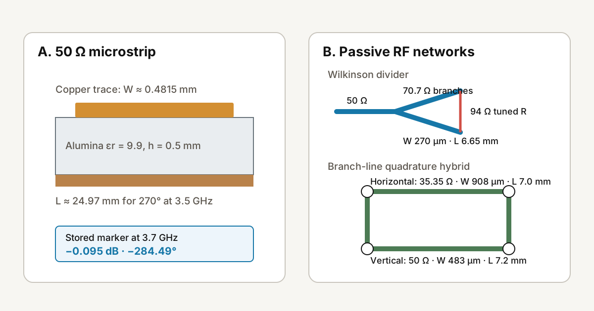
<p>I began by collecting the shared assumptions from my RF coursework: a 0.5 mm alumina substrate, relative permittivity 9.9, and a 3.5 GHz design frequency. Those values set the microstrip width, guided wavelength, and quarter-wave sections used by both passive networks.</p>

<figure>
  <img src="/assets/images/learning/coursework/rf-passive-microstrip-divider-hybrid.svg" alt="Alumina microstrip and stored 3.7 GHz marker beside Wilkinson and branch-line dimensions" width="1200" height="630" />
  <figcaption>The left panel keeps the transmission-line calculation together; the right panel compares the dimensions entered for the two networks.</figcaption>
</figure>

<h2 id="microstrip">Width and length</h2>

<p>The calculated width for a 50 Ω line was about 0.4815 mm. A 270° delay at 3.5 GHz is three quarters of the guided wavelength, giving a length near 24.97 mm. I initially confused the free-space wavelength with the shorter guided wavelength on alumina; separating them made the report value consistent.</p>

<figure>
  <table>
    <thead><tr><th>Item</th><th>Value</th><th>Use</th></tr></thead>
    <tbody>
      <tr><td>Relative permittivity</td><td>9.9</td><td>Alumina</td></tr>
      <tr><td>Substrate height</td><td>0.5 mm</td><td>Shared condition</td></tr>
      <tr><td>50 Ω width</td><td>about 0.4815 mm</td><td>Microstrip calculation</td></tr>
      <tr><td>270° length</td><td>about 24.97 mm</td><td>at 3.5 GHz</td></tr>
    </tbody>
  </table>
  <figcaption>I converted µm and mm values to one unit before comparing the designs.</figcaption>
</figure>

<h2 id="marker">Reading the 3.7 GHz marker</h2>

<p>A stored Cadence screen marks approximately −0.095 dB insertion loss and −284.49° phase at 3.7 GHz. The accumulated phase is larger than the 270° target at 3.5 GHz, which is consistent with observing the same line at a higher frequency. These are values read from the earlier simulation screen, not instrument measurements.</p>

<h2 id="wilkinson">Wilkinson divider</h2>

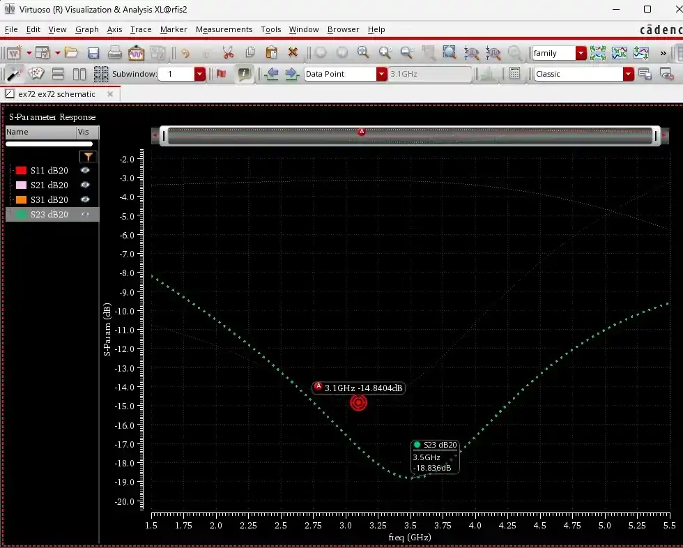
<p>An equal-split Wilkinson uses two theoretical 70.7 Ω quarter-wave branches. The stored design tuned the resistor from 100 Ω to 94 Ω and used branch width 270 µm and length 6.65 mm. The screen places S21 and S31 near −3 dB and S11 near −15 dB. I treat the notch position and center-frequency alignment as items to check again instead of describing the match as perfect.</p>

<figure><img src="/assets/images/study/coursework/high-frequency-wilkinson.webp" alt="Saved Cadence S-parameter view with S11, S21, S31, and S23 traces" width="980" height="784" /><figcaption>I read the split and matching markers together on the saved screen.</figcaption></figure>

<figure>
  <table>
    <thead><tr><th>Network</th><th>Transmission line</th><th>Reading from stored screen</th></tr></thead>
    <tbody>
      <tr><td>Wilkinson</td><td>70.7 Ω, W 270 µm, L 6.65 mm</td><td>S21/S31 near −3 dB, S11 near −15 dB</td></tr>
      <tr><td>Branch-line</td><td>35.35 Ω horizontal, 50 Ω vertical</td><td>center shift in split and isolation curves</td></tr>
    </tbody>
  </table>
  <figcaption>Keeping theoretical impedance and entered geometry in separate columns made the tuning step easier to follow.</figcaption>
</figure>

<h2 id="hybrid">Branch-line hybrid</h2>

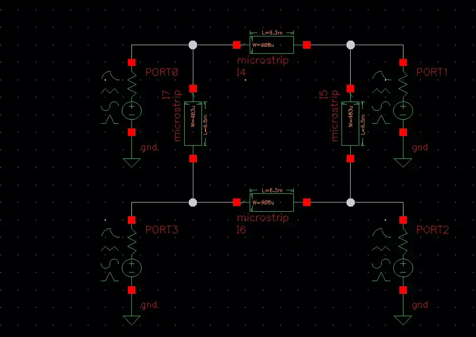
<p>The quadrature hybrid forms a rectangle with 35.35 Ω horizontal lines and 50 Ω vertical lines. The stored dimensions were W 908 µm and L 7.0 mm horizontally, then W 483 µm and L 7.2 mm vertically. Drawing the two widths separately helped me remember why the four sides do not share one impedance.</p>

<figure><img src="/assets/images/study/coursework/high-frequency-hybrid.webp" alt="Saved branch-line hybrid schematic with four ports and different horizontal and vertical microstrip widths" width="980" height="657" /><figcaption>The saved Cadence schematic makes the port order and four line sections visible.</figcaption></figure>

<h2 id="interpretation">Simulation-only interpretation</h2>

<p>This note connects calculations in the report to earlier Cadence screens. I did not rerun the netlist or measure a fabricated network with a VNA. My next step is to recreate the same sweep and inspect marker frequency, port definitions, and dB conventions together.</p>

<h2 id="navigation">Previous and next</h2>

<ul>
  <li><a href="/en/coursework/">Previous: coursework overview</a></li>
  <li><a href="/en/blog/series/rf-microwave/">Series: RF and Microwave</a></li>
  <li><a href="/en/blog/2026/07/31/radar-candidate-timing/">Next: FMCW radar candidate timing</a></li>
</ul>]]></content><author><name>Hyeongrok Ryu</name></author><category term="microstrip" /><category term="cadence-virtuoso" /><category term="wilkinson-divider" /><category term="branch-line-hybrid" /><summary type="html"><![CDATA[My review of alumina microstrip calculations and stored Cadence divider and hybrid screens.]]></summary><media:thumbnail xmlns:media="http://search.yahoo.com/mrss/" url="https://dororok9061.github.io/assets/images/og.jpg" /><media:content medium="image" url="https://dororok9061.github.io/assets/images/og.jpg" xmlns:media="http://search.yahoo.com/mrss/" /></entry><entry xml:lang="ko"><title type="html">3.5 GHz Microstrip에서 Wilkinson·Branch-Line까지</title><link href="https://dororok9061.github.io/blog/2026/08/01/rf-passive-microstrip-divider-hybrid/" rel="alternate" type="text/html" title="3.5 GHz Microstrip에서 Wilkinson·Branch-Line까지" /><published>2026-08-01T11:02:00+09:00</published><updated>2026-08-01T11:02:00+09:00</updated><id>https://dororok9061.github.io/blog/2026/08/01/rf-passive-microstrip-divider-hybrid-ko</id><content type="html" xml:base="https://dororok9061.github.io/blog/2026/08/01/rf-passive-microstrip-divider-hybrid/"><![CDATA[<h2 id="start">3.5 GHz 조건부터</h2>

<p>고주파공학 과제를 다시 보면서 먼저 공통 조건을 한 줄에 모았다. 기판은 두께 0.5 mm, 상대유전율 9.9인 alumina이고 설계 중심주파수는 3.5 GHz였다. 이 조건이 microstrip 폭과 유도파장, divider와 hybrid의 λ/4 길이를 모두 결정한다.</p>

<figure>
  <img src="/assets/images/learning/coursework/rf-passive-microstrip-divider-hybrid.svg" alt="왼쪽에는 alumina 50옴 microstrip과 3.7 GHz marker가 있고 오른쪽에는 Wilkinson divider와 branch-line hybrid 치수가 있다" width="1200" height="630" />
  <figcaption>한쪽에는 전송선 계산을, 다른 쪽에는 두 수동 분배 회로의 실제 입력 치수를 배치했다.</figcaption>
</figure>

<h2 id="microstrip">폭과 길이 계산</h2>

<p>50 Ω 조건으로 계산한 선폭은 약 0.4815 mm였다. 3.5 GHz에서 270° 위상지연은 유도파장의 3/4이므로 길이는 약 24.97 mm가 된다. 처음에는 자유공간 파장을 그대로 넣었지만, alumina 위에서 짧아진 유도파장을 써야 보고서 길이와 맞았다.</p>

<figure>
  <table>
    <thead><tr><th>항목</th><th>값</th><th>메모</th></tr></thead>
    <tbody>
      <tr><td>상대유전율</td><td>9.9</td><td>Alumina</td></tr>
      <tr><td>기판 두께</td><td>0.5 mm</td><td>공통 조건</td></tr>
      <tr><td>50 Ω 선폭</td><td>약 0.4815 mm</td><td>Microstrip 계산</td></tr>
      <tr><td>270° 선로 길이</td><td>약 24.97 mm</td><td>3.5 GHz 기준</td></tr>
    </tbody>
  </table>
  <figcaption>단위가 µm와 mm로 섞여 있어 모든 값을 mm 기준으로 먼저 비교했다.</figcaption>
</figure>

<h2 id="marker">3.7 GHz marker 읽기</h2>

<p>저장된 Cadence 화면의 3.7 GHz marker에는 insertion loss가 약 −0.095 dB, 위상이 약 −284.49°로 표시되어 있었다. 목표 3.5 GHz의 270°보다 주파수가 높아지면서 위상 누적도 더 커진 것으로 읽었다. 이 값은 당시 simulation 화면에서 옮긴 값이며 장비로 잰 수치는 아니다.</p>

<h2 id="wilkinson">Wilkinson divider</h2>

<p>동일 분배 Wilkinson의 두 λ/4 branch는 이론상 약 70.7 Ω이다. 저장된 설계에서는 저항을 100 Ω에서 94 Ω로 조정했고, branch 폭 270 µm와 길이 6.65 mm를 사용했다. 화면에서 S21과 S31은 약 −3 dB, S11은 약 −15 dB 수준이었다. 나는 이 수치를 완벽한 정합이라고 부르기보다 중심주파수와 notch 위치를 다시 확인해야 하는 simulation 결과로 읽었다.</p>

<figure><img src="/assets/images/study/coursework/high-frequency-wilkinson.webp" alt="S11과 S21, S31, S23 곡선이 표시된 Wilkinson divider Cadence 화면" width="980" height="784" /><figcaption>저장된 S-parameter 화면에서 분배와 정합 marker를 함께 읽었다.</figcaption></figure>

<figure>
  <table>
    <thead><tr><th>회로</th><th>전송선</th><th>저장된 화면에서 읽은 값</th></tr></thead>
    <tbody>
      <tr><td>Wilkinson</td><td>70.7 Ω, W 270 µm, L 6.65 mm</td><td>S21·S31 약 −3 dB, S11 약 −15 dB</td></tr>
      <tr><td>Branch-Line</td><td>수평 35.35 Ω, 수직 50 Ω</td><td>분배·격리 곡선의 중심 이동 확인</td></tr>
    </tbody>
  </table>
  <figcaption>이론 임피던스와 입력한 물리 치수를 따로 적어야 tuning 과정을 설명하기 쉬웠다.</figcaption>
</figure>

<h2 id="hybrid">Branch-Line hybrid</h2>

<p>Quadrature hybrid는 위아래 수평선에 35.35 Ω, 좌우 수직선에 50 Ω를 배치한 사각형 구조였다. 저장된 치수는 수평선 W 908 µm, L 7.0 mm, 수직선 W 483 µm, L 7.2 mm였다. 두 종류의 선폭을 바꿔 그리면 왜 네 변이 같은 임피던스가 아닌지 바로 보였다.</p>

<figure><img src="/assets/images/study/coursework/high-frequency-hybrid.webp" alt="네 개 port와 서로 다른 폭의 수평·수직 microstrip으로 구성한 branch-line hybrid 회로" width="980" height="657" /><figcaption>직접 저장한 Cadence 회로 화면에서 port와 네 선로의 배치를 확인했다.</figcaption></figure>

<h2 id="interpretation">Simulation으로만 해석</h2>

<p>이번 글에서는 보고서 계산과 당시 Cadence 화면을 연결했다. 새 netlist를 실행하거나 VNA로 제작 회로를 측정하지 않았다. 다음에는 동일한 주파수 sweep 조건을 다시 만들고 marker, port 정의, dB 기준을 한 화면에서 확인할 생각이다.</p>

<h2 id="navigation">이전 글과 다음 글</h2>

<ul>
  <li><a href="/coursework/">이전: 전공과목 전체 보기</a></li>
  <li><a href="/blog/series/rf-microwave/">시리즈: RF · Microwave</a></li>
  <li><a href="/blog/2026/07/31/radar-candidate-timing/">다음: FMCW Radar 후보 시점 정리</a></li>
</ul>]]></content><author><name>Hyeongrok Ryu</name></author><category term="microstrip" /><category term="cadence-virtuoso" /><category term="wilkinson-divider" /><category term="branch-line-hybrid" /><summary type="html"><![CDATA[Alumina microstrip 계산과 저장된 Cadence divider·hybrid 화면을 수치와 회로 구조로 다시 읽은 기록.]]></summary><media:thumbnail xmlns:media="http://search.yahoo.com/mrss/" url="https://dororok9061.github.io/assets/images/og.jpg" /><media:content medium="image" url="https://dororok9061.github.io/assets/images/og.jpg" xmlns:media="http://search.yahoo.com/mrss/" /></entry><entry xml:lang="en"><title type="html">Reading the Mealy 101 Detector and 8-to-1 MUX Sources</title><link href="https://dororok9061.github.io/en/blog/2026/08/01/controller-logic-mealy-mux/" rel="alternate" type="text/html" title="Reading the Mealy 101 Detector and 8-to-1 MUX Sources" /><published>2026-08-01T11:01:00+09:00</published><updated>2026-08-01T11:01:00+09:00</updated><id>https://dororok9061.github.io/en/blog/2026/08/01/controller-logic-mealy-mux-en</id><content type="html" xml:base="https://dororok9061.github.io/en/blog/2026/08/01/controller-logic-mealy-mux/"><![CDATA[<h2 id="source">Starting from source</h2>

<p>I reopened the stored <code>mealy.vhd</code>, <code>mealy_tb.vhd</code>, and <code>mux_8to1.vhd</code> files from my 2024 coursework. I focused on the entity, architecture, and stimulus that I had written instead of the Vivado cache and generated executables.</p>

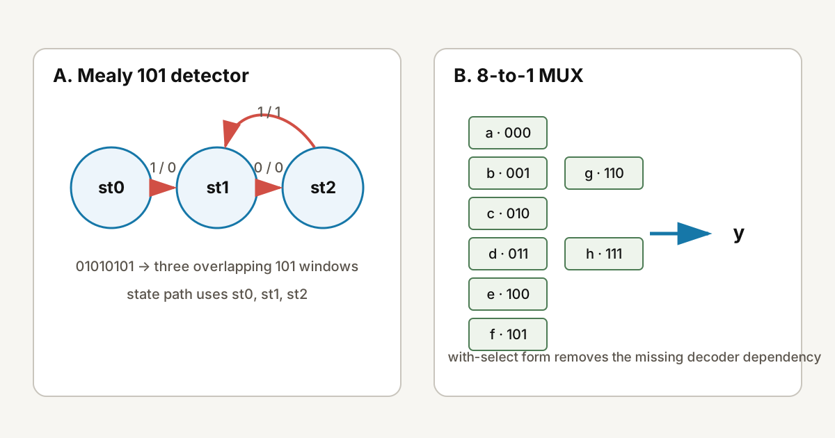
<figure>
  <img src="/assets/images/learning/coursework/controller-logic-mealy-mux.svg" alt="Three-state overlapping Mealy 101 detector beside an eight-input multiplexer selection map" width="1200" height="630" />
  <figcaption>The left panel traces the overlapping detector; the right panel rewrites the same selection function without a decoder dependency.</figcaption>
</figure>

<h2 id="states">Finding 101 with three states</h2>

<p>The transition path uses three states. <code>st0</code> has no useful prefix, <code>st1</code> means the latest bit is 1, and <code>st2</code> means the latest two bits are 10. A 1 in <code>st2</code> completes 101 and asserts <code>dout</code>. Returning to <code>st1</code> preserves that final 1 as the start of an overlapping pattern.</p>

<figure>
  <table>
    <thead><tr><th>Current state</th><th>Input 0</th><th>Input 1</th><th>Output 1</th></tr></thead>
    <tbody>
      <tr><td>st0</td><td>st0</td><td>st1</td><td>-</td></tr>
      <tr><td>st1</td><td>st2</td><td>st1</td><td>-</td></tr>
      <tr><td>st2</td><td>st2</td><td>st1</td><td>on input 1</td></tr>
    </tbody>
  </table>
  <figcaption>The <code>st2 → st1</code> transition is the step that keeps overlapping detections possible.</figcaption>
</figure>

<h2 id="stimulus">Tracing 01010101</h2>

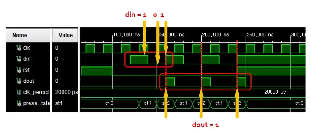
<p>The stored testbench deasserts reset and applies <code>01010101</code> at 20 ns intervals. Following the table by hand completes 101 at the fourth, sixth, and eighth input positions. I did not rerun GHDL or Vivado simulation while writing this note, so these are source-level expectations rather than a new waveform result.</p>

<figure><img src="/assets/images/study/coursework/controller-logic-waveform.webp" alt="Saved waveform showing 01010101 input, st0 st1 st2 states, and dout pulses" width="1200" height="514" /><figcaption>I followed the saved input and state transitions together.</figcaption></figure>

<h2 id="mux">Writing a standalone MUX</h2>

<p>The original <code>mux_8to1.vhd</code> instantiates a <code>dec_3to8</code> component and combines decoded lines with AND and OR gates. The decoder source was not present in the stored bundle I reviewed. I therefore rewrote the same truth table as a dependency-free study example.</p>

<figure>
  <pre><code class="language-vhdl">with sel select
  y &lt;= a when "000",
       b when "001",
       c when "010",
       d when "011",
       e when "100",
       f when "101",
       g when "110",
       h when others;</code></pre>
  <figcaption>This example explains the selection function; it does not alter or prove a build of the archived project.</figcaption>
</figure>

<h2 id="rerun">What I will check next</h2>

<p>On the next run I will place <code>present_state</code>, <code>next_state</code>, and <code>dout</code> beside the input at each clock edge. For the MUX, I will exercise all select values on the standalone version first and compare the structural version only after recovering its decoder source.</p>

<h2 id="navigation">Previous and next</h2>

<ul>
  <li><a href="/en/coursework/">Previous: coursework overview</a></li>
  <li><a href="/en/blog/series/vhdl-foundations/">Series: VHDL Digital Logic Foundations</a></li>
  <li><a href="/en/blog/2026/07/31/fpga-architecture-equivalence/">Next: shift-register and circular-queue verification</a></li>
</ul>]]></content><author><name>Hyeongrok Ryu</name></author><category term="vhdl" /><category term="mealy-fsm" /><category term="sequence-detector" /><category term="multiplexer" /><summary type="html"><![CDATA[My source-level review of overlapping 101 transitions and a decoder-based multiplexer from stored VHDL coursework.]]></summary><media:thumbnail xmlns:media="http://search.yahoo.com/mrss/" url="https://dororok9061.github.io/assets/images/og.jpg" /><media:content medium="image" url="https://dororok9061.github.io/assets/images/og.jpg" xmlns:media="http://search.yahoo.com/mrss/" /></entry><entry xml:lang="ko"><title type="html">Mealy 101 검출기와 8-to-1 MUX 소스 다시 읽기</title><link href="https://dororok9061.github.io/blog/2026/08/01/controller-logic-mealy-mux/" rel="alternate" type="text/html" title="Mealy 101 검출기와 8-to-1 MUX 소스 다시 읽기" /><published>2026-08-01T11:01:00+09:00</published><updated>2026-08-01T11:01:00+09:00</updated><id>https://dororok9061.github.io/blog/2026/08/01/controller-logic-mealy-mux-ko</id><content type="html" xml:base="https://dororok9061.github.io/blog/2026/08/01/controller-logic-mealy-mux/"><![CDATA[<h2 id="source">소스에서 다시 시작</h2>

<p>이번에는 2024년에 저장한 <code>mealy.vhd</code>, <code>mealy_tb.vhd</code>, <code>mux_8to1.vhd</code>를 차례로 읽었다. Vivado가 만든 cache와 실행 파일보다 직접 작성한 entity, architecture, testbench 입력을 먼저 봤다.</p>

<figure>
  <img src="/assets/images/learning/coursework/controller-logic-mealy-mux.svg" alt="왼쪽은 st0, st1, st2로 구성한 Mealy 101 검출기이고 오른쪽은 3-bit 선택값에 따른 8-to-1 MUX 입력표" width="1200" height="630" />
  <figcaption>왼쪽 패널은 overlapping 101 검출기, 오른쪽 패널은 같은 선택 논리를 독립형 MUX로 다시 적은 모습이다.</figcaption>
</figure>

<h2 id="states">세 상태로 101 찾기</h2>

<p>상태 이름은 단순했다. <code>st0</code>는 아직 유효한 앞부분이 없고, <code>st1</code>은 마지막 입력이 1이며, <code>st2</code>는 마지막 두 입력이 10인 상태다. <code>st2</code>에서 1을 받으면 101이 완성되어 <code>dout</code>이 1이 된다. 동시에 <code>st1</code>로 돌아가므로 마지막 1을 다음 패턴의 첫 1로 다시 쓸 수 있다.</p>

<figure>
  <table>
    <thead><tr><th>현재 상태</th><th>입력 0</th><th>입력 1</th><th>출력 1 조건</th></tr></thead>
    <tbody>
      <tr><td>st0</td><td>st0</td><td>st1</td><td>-</td></tr>
      <tr><td>st1</td><td>st2</td><td>st1</td><td>-</td></tr>
      <tr><td>st2</td><td>st2</td><td>st1</td><td>입력 1</td></tr>
    </tbody>
  </table>
  <figcaption>상태표를 만들자 overlap 처리가 <code>st2 → st1</code> 전이에 들어 있다는 점이 보였다.</figcaption>
</figure>

<h2 id="stimulus">01010101 따라가기</h2>

<p>저장된 testbench는 reset을 내린 뒤 <code>01010101</code>을 20 ns 간격으로 넣는다. 상태표대로 종이에 따라가면 네 번째, 여섯 번째, 여덟 번째 입력에서 101이 완성된다. 이 계산은 코드의 전이 규칙을 손으로 확인한 것이며, 이번 정리에서 GHDL이나 Vivado simulation을 다시 돌리지는 않았다.</p>

<figure><img src="/assets/images/study/coursework/controller-logic-waveform.webp" alt="01010101 입력과 st0, st1, st2 상태, dout pulse가 표시된 저장 파형" width="1200" height="514" /><figcaption>당시 저장한 파형에서 입력과 상태 전이를 함께 따라갔다.</figcaption></figure>

<h2 id="mux">MUX를 독립형으로 쓰기</h2>

<p>원래 <code>mux_8to1.vhd</code>는 <code>dec_3to8</code> component와 AND/OR 조합으로 8개 입력을 선택한다. 저장 묶음에서는 decoder의 VHDL 원본을 찾지 못했다. 그래서 같은 진리표를 공부할 때는 의존성이 없는 <code>with select</code> 형태로 다시 적어봤다.</p>

<figure>
  <pre><code class="language-vhdl">with sel select
  y &lt;= a when "000",
       b when "001",
       c when "010",
       d when "011",
       e when "100",
       f when "101",
       g when "110",
       h when others;</code></pre>
  <figcaption>이 예시는 원래 archive를 고쳤다는 뜻이 아니라, 같은 선택 함수를 독립된 VHDL로 표현한 학습용 코드다.</figcaption>
</figure>

<h2 id="rerun">다시 실행할 때 볼 것</h2>

<p>다음 실행에서는 clock edge 직후의 <code>present_state</code>, 조합논리의 <code>next_state</code>, <code>dout</code>을 한 파형에 놓을 생각이다. MUX는 먼저 독립형 예제를 모든 선택값으로 확인한 뒤, decoder 원본을 다시 찾으면 구조형 구현과 출력을 비교할 예정이다.</p>

<h2 id="navigation">이전 글과 다음 글</h2>

<ul>
  <li><a href="/coursework/">이전: 전공과목 전체 보기</a></li>
  <li><a href="/blog/series/vhdl-foundations/">시리즈: VHDL 디지털논리 기초</a></li>
  <li><a href="/blog/2026/07/31/fpga-architecture-equivalence/">다음: Shift Register와 Circular Queue 검증 글</a></li>
</ul>]]></content><author><name>Hyeongrok Ryu</name></author><category term="vhdl" /><category term="mealy-fsm" /><category term="sequence-detector" /><category term="multiplexer" /><summary type="html"><![CDATA[저장된 VHDL에서 overlapping 101 상태전이와 decoder 기반 MUX 구조를 다시 따라간 기록.]]></summary><media:thumbnail xmlns:media="http://search.yahoo.com/mrss/" url="https://dororok9061.github.io/assets/images/og.jpg" /><media:content medium="image" url="https://dororok9061.github.io/assets/images/og.jpg" xmlns:media="http://search.yahoo.com/mrss/" /></entry></feed>